
81 - 90 of 311
inp semiconductor substrate wafers
Selling leads
|
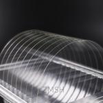
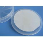
...₂). The unique properties of quartz make it an essential material in various high-tech industries. Quartz wafers exhibit excellent characteristics ...
2025-07-10 18:23:14
|
|
... wafer is a specialized type of wafer that combines the properties of silicon carbide and silicon materials. The wafer consists of a layer of semi...
2025-05-06 20:45:23
|
|
2inch 3inch 4inch InAs Wafer Crystal Substrates N-Type For MBE 99.9999% Monocrystalline Introduce of InAs substrate Indium InAs or indium mono...
2025-05-06 20:44:58
|
|
... 6inch dia 150mm silicon carbide single crystal (sic) substrates wafers, sic crystal ingots sic semiconductor substrates,Silicon Carbide crystal ...
2025-05-06 20:40:44
|
|
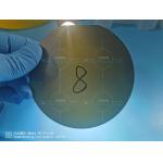
...substrates template,GaN wafer for LeD,semiconducting Gallium Nitride Wafer for ld,GaN template, mocvd GaN Wafer,Free-standing GaN Substrates by ...
2025-05-06 20:44:29
|
|
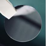
...wafer 4inch Polished CZ Dopant Arsenic(As) Boron(B) Phosphorus(Ph) (100) Semiconductor Describe of Si Wafer: A Silicon wafer is a very thin round ...
2025-05-06 20:45:29
|
|
...substrates wafers, sic crystal ingots sic semiconductor substrates,Silicon Carbide crystal Wafer/ Customzied as-cut sic wafers 4inch 2inch 6inch ...
2025-05-06 20:40:47
|
|
... technologies and the-state-of-the art PVT growth reactors and facilities to fabricate different sizes of high-quality single crystalline AlN ...
2025-05-06 20:44:44
|
|
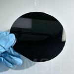
... to a silicon carbide (SiC) wafer with a 12-inch diameter (approximately 300mm), a size standard used in the semiconductor industry for the mass ...
2025-05-06 20:41:54
|
|
.... Featuring a thickness ranging from 10μm to 25μm, this crucial substrate is available in 6-inch and 8-inch diameters, ensuring versatility for ...
2025-05-06 20:45:05
|