
71 - 80 of 311
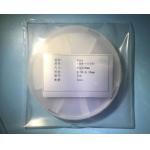
inp semiconductor substrate wafers
Selling leads
|
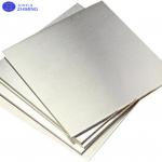
...advanced materials research and applications due to their unique physical properties, such as lightweight and excellent thermal conductivity. These ...
2025-05-06 20:45:46
|
|
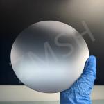
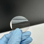
... substrate sapphire window sapphire wafer Applications of AlN template Silicon-based semiconductor technology has reached its limits and could not ...
2025-05-06 20:44:39
|
|
Silicon wafer Conductivity Solar Cells Solar Cells Power Semiconductor Devices High Purity Product Description: Attributes Details Substrate Material ...
2025-05-06 20:45:09
|
|
...Wafer Si Substrate 111 P Type N Type for Micro-electromechanical systems (MEMS) Or Power semiconductor devices Or Optical components and sensors ...
2025-05-06 20:45:50
|
|
... arsenide GaAs Wafer Product Description Our 2’’ to 6’’ semi-conducting & semi-insulating GaAs crystal & wafer are wildly used in semiconductor ...
2025-05-06 20:44:32
|
|
... arsenide GaAs Wafer Product Description Our 2’’ to 6’’ semi-conducting & semi-insulating GaAs crystal & wafer are wildly used in semiconductor ...
2025-05-06 20:44:52
|
|
... for semiconductor devices. Their exceptional electrical conductivity properties, which can be precisely modified through doping with elements like ...
2025-05-06 20:45:58
|
|
... stations powering 5G networks, and integrated into tools manufacturing next-gen microchips, quartz wafers are essential. These high-purity ...
2025-07-10 18:23:13
|
|
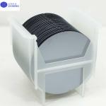
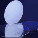
...substrate wafer, ZMSH offers the best price on the market for 2 inch and 3 inch Research grade Silicon Carbide substrate wafers. The SiC substrate ...
2025-07-22 00:12:04
|
|
...Wafer 4H/6H-P Silicon Carbide Substrate DSP (111) Semiconductor RF Microwave LED Lasers Description of SiC Wafer: The 6-inch P-Type Silicon Carbide ...
2025-05-06 20:41:42
|