
1 - 10 of 311
inp semiconductor substrate wafers
Selling leads
|
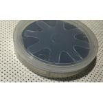
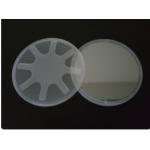
2inch InP wafers 3inch 4inch N/P TYPE InP Semiconductor Substrate Wafers Doped S+/ Zn+ /Fe + growth (modified VFG method) is used to pull a single ...
2025-05-06 20:44:36
|

|
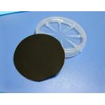
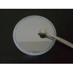
.../3 inch/4 inch 350-650 um InP Crystal Wafer Dummy Prime Semiconductor Substrate Shanghai Xinkehui New Materials Co. Ltd. We specialize in ...
2025-07-18 00:09:54
|
|
2inch InP wafers 3inch 4inch N/P TYPE InP Semiconductor Substrate Wafers Doped S+/ Zn+ /Fe + growth (modified VFG method) is used to pull a single ...
2025-05-06 20:44:37
|
|
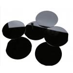
2inch/3inch/4inch S/Fe/Zn doped InP Indium Phosphide Single Crystal Wafer Indium phosphide (InP) is an important compound semiconductor material with ...
2025-05-06 20:44:34
|
|
...InP (Indium Phosphide) semiconductor wafers, renowned for their exceptional electronic and optoelectronic properties, have found extensive ...
2025-05-06 20:44:23
|
|
... Wafer Product Description (GaAs) Gallium Arsenide Wafers PWAM Develops and manufactures compound semiconductor substrates-gallium arsenide crystal ...
2025-05-06 20:44:31
|
|
*, *::before, *::after {box-sizing: border-box;}* {margin: 0;}html, body {height: 100%;}body {line-height: 1.5;-webkit-font-smoothing: antialiased;...
2025-05-06 20:45:37
|
|
...Wafer Semiconductor Substrate For Epitaxial Growth VGF 2inch 4inch 6inch n-type prime grade GaAs wafer for epitaxial growth Gallium arsenide can be ...
2025-05-06 20:45:00
|
|
4inch diameter 100mm Lithium niobate LiNbO3 substrate wafer, LN wafer for saw and optical,SAW Grade LiNbO3 Crystal ingot Description: Lithium niobate ...
2025-05-06 20:44:35
|
|
... Substrate Indium Arsenide InAs wafer Application Indium Arsenide (InAs) single crystal semiconductor substrates are materials with unique ...
2025-07-18 00:09:54
|