
11 - 20 of 311
inp semiconductor substrate wafers
Selling leads
|
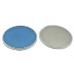
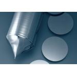
2INCH dia50.8mm Ga doped Ge substrate 4inch N-type 500um Ge wafers Ge wafer for microelectronic application N type, Sb doped Ge wafer N type,undoped ...
2025-05-06 20:44:46
|
|
...wafer for epitaxial growth GaAs wafer (Gallium Arsenide) is an advantageous alternative to silicon that has been evolving in the semiconductor ...
2025-05-06 20:44:45
|
|
...Substrate/Wafers (150mm, 200mm) Silicon Carbide Ceramic Excellent CorrosionSingle crystal single side polished silicon wafer sic wafer polishing ...
2025-05-06 20:41:07
|
|
...)Crystal Silicon carbide (SiC), also known as carborundum, is a semiconductor containing silicon and carbon with chemical formula SiC. SiC is used ...
2025-05-06 20:42:00
|
|
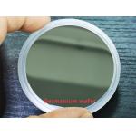
...germanium wafers, which is short for Ge wafers grown by VGF / LEC. Lightly doped P and N-type Germanium wafers can be also used for the Hall effect ...
2025-05-06 20:44:50
|
|
...Substrates Wafer DSP Notch High Precision 8inch/6inch/5inch/ 2inch /3inch 4inch /5inch C-axis/ a-axis/ r-axis/ m-axis 6"/6inch dia150mm C-plane ...
2025-05-06 20:39:17
|
|
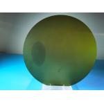
... (GaAs) Gallium Arsenide Wafers Gallium arsenide (GaAs) is a compound of the elements gallium and arsenic. It is a III-V direct bandgap semiconduct...
2025-05-06 20:44:31
|
|
... (GaAs) Gallium Arsenide Wafers Gallium arsenide (GaAs) is a compound of the elements gallium and arsenic. It is a III-V direct bandgap semiconduct...
2025-05-06 20:44:43
|
|
...wafers Germanium substrate Ge window for infrared Co2 lasers Ge Material Introduce Among optical materials, germanium materials are increasingly ...
2025-05-06 20:44:48
|
|
2inch/3inch/4inch/6inch Y-42°/36°/128° LT Lithium tantalate (LiTaO3) crystal / Fe+ doped type 250um/300um substrate wafer Product Name:Lithium ...
2025-05-06 20:44:34
|