
41 - 50 of 311
inp semiconductor substrate wafers
Selling leads
|
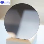
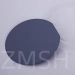
InP DFB Epiwafer wavelength 1390nm InP substrate 2 4 6 inch for 2.5~25G DFB laser diode InP DFB Epiwafer InP substrate's brief InP DFB Epiwafers ...
2025-05-06 20:45:38
|
|
... innovation. Crafted from pristine indium phosphide, a binary semiconductor renowned for its superior electron velocity, our wafer offers ...
2025-05-06 20:45:10
|
|
...variety of applications in the telecommunications, optoelectronics, and semiconductor industries. With superior optical and electronic properties, ...
2025-05-06 20:45:10
|
|
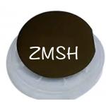
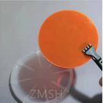
...InP substrate dia 2 3 4 6 inch thickness:350-650um InGaAs doping FP(Fabry-Perot)) Epiwafer InP substrate's abstract Fabry-Perot (FP) Epiwafer on ...
2025-05-06 20:45:36
|
|
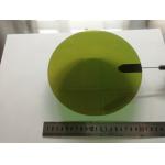
InP wafer 2inch 3inch 4inch VGF P type N type Depant Zn S Fe Undoped Prime Grade Testing Grade *, *::before, *::after {box-...
2025-05-06 20:45:30
|
|
...wafer 2inch with OF Location/Length EJ 0-1-1 / 16±1mm LED LD Mobility Min 100 Product Description: A GaP wafer is a semiconductor substrate ...
2025-05-06 20:45:06
|
|
...InP (Indium Phosphide) wafers are renowned for their low defect density and high performance, widely used in optoelectronics and microelectronics. ...
2025-05-06 20:44:24
|
|
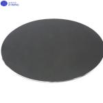
...Substrate / Silicon Carbide Ceramic Excellent CorrosionSingle crystal single side polished silicon wafer sic wafer polishing wafer manufacturer ...
2025-05-06 20:42:00
|
|
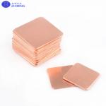
... to deliver optimal electrical and thermal performance for advanced semiconductor and electronic applications. These wafers are available in ...
2025-05-06 20:45:45
|
|
...Wafer with (111) Crystal Orientation – Introduction The 8-inch silicon wafer with (111) crystal orientation is a vital component in the semiconduct...
2025-05-06 20:45:52
|