
91 - 100 of 311
inp semiconductor substrate wafers
Selling leads
|
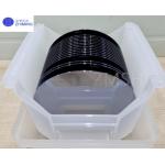
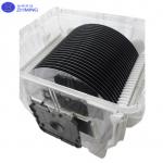
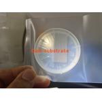
...wafer P Type N Type 6 inch 8 inch 12 inch Surface polish SSP/DSP Abstract of SOI wafer Silicon on Insulator (SOI) is an advanced semiconductor ...
2025-05-06 20:45:55
|
|
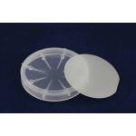
...wafers Germanium substrate Ge window for infrared Co2 lasers Ge Material Introduce Among optical materials, germanium materials are increasingly ...
2025-05-06 20:44:49
|
|
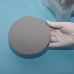
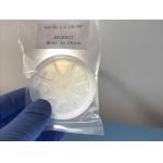
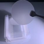
... as the foundation for high-performance semiconductor devices. Crafted with advanced float-zone mono-crystalline silicon technology, this substrate ...
2025-05-06 20:45:11
|
|
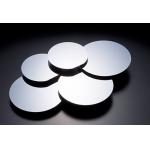
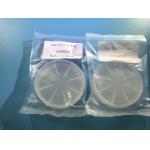
...wafer CZ 200mm Prime Grade Silicon Wafer , SSP,DSP P type,B dopant,for semiconducter matrial Product Introduction: 8-Inch (200mm) Prime Grade ...
2025-05-06 20:45:53
|
|
...substrates template,GaN wafer for LeD,semiconducting Gallium Nitride Wafer for ld,GaN template, mocvd GaN Wafer,Free-standing GaN Substrates by ...
2025-05-06 20:44:12
|
|
...substrates template,GaN wafer for LeD,semiconducting Gallium Nitride Wafer for ld,GaN template, mocvd GaN Wafer,Free-standing GaN Substrates by ...
2025-05-06 20:44:13
|
|
...substrates template,GaN wafer for LeD,semiconducting Gallium Nitride Wafer for ld,GaN template, mocvd GaN Wafer,Free-standing GaN Substrates by ...
2025-05-06 20:44:28
|
|
...substrates template,GaN wafer for LeD,semiconducting Gallium Nitride Wafer for ld,GaN template, mocvd GaN Wafer,Free-standing GaN Substrates by ...
2025-05-06 20:44:15
|
|
...substrates template,GaN wafer for LeD,semiconducting Gallium Nitride Wafer for ld,GaN template, mocvd GaN Wafer,Free-standing GaN Substrates by ...
2025-05-06 20:44:20
|
|
..., optoelectronic devices, semiconductor devices, and other fields. The high light transmittance and high hardness of sapphire wafers make them ...
2025-07-20 00:12:23
|