
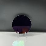
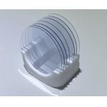
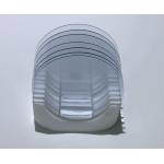
Single Crystal Monocrystal Semiconductor Substrate Indium Arsenide InAs Substrate
|
|
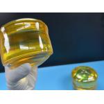
2-4inch Gallium antimonide GaSb Substrate Single Crystal
Monocrystal for Semiconductor 1. High-Performance Infrared DetectorsDue to its narrow bandgap, InAs substrates are ideal for manufacturing high-performance infrared detectors, particularly in the mid-infrared and long-wavelength infrared ranges. These detectors are essential in applications such as night vision, thermal imaging, and environmental monitoring. 2. Quantum Dot TechnologyInAs is used in the fabrication of quantum dots, which are critical for developing advanced optoelectronic devices like quantum dot lasers, quantum computing systems, and high-efficiency solar cells. Its superior electron mobility and quantum confinement effects make it a prime candidate for next-generation semiconductor devices. 3. High-Speed ElectronicsInAs substrates offer excellent electron mobility, making them suitable for high-speed electronics, such as high-frequency transistors (HEMTs) and high-speed integrated circuits used in telecommunications and radar systems. 4. Optoelectronic DevicesInAs is a popular material for fabricating optoelectronic devices, such as lasers and photodetectors, due to its direct bandgap and high electron mobility. These devices are critical for applications in fiber-optic communication, medical imaging, and spectroscopy. 5. Thermoelectric DevicesInAs's superior thermoelectric properties make it a promising
candidate for thermoelectric generators and coolers, which are used
to convert temperature gradients into electrical energy and for
cooling applications in electronics.
InAs Product Specification
Electrical and Doping Specification
Q: Are you trading company or manufacturer ?A: zmkj is a trading company but have a sapphire manufacturer |
||||||||||||||||||||||||||||||||||||||||||||||||||||||||||||||||||||||||||||||||||||||||||||||||||||||||||||
| Product Tags: Monocrystal Semiconductor Substrate Single Crystal Indium Phosphide Wafer Semiconductor InAs Substrate | ||||||||||||||||||||||||||||||||||||||||||||||||||||||||||||||||||||||||||||||||||||||||||||||||||||||||||||
|
Semi Insulating GaN-On-Silicon Wafer Free Standing Gallium Nitride Substrates |
|
1inch 2inch Beta Coefficient Ga2O3 Gallium Oxide Wafer Substrate Dsp Ssp |
|
Beta Coefficient-Ga2O3 Gallium Oxide Wafer Doped Mg Fe3+ Square Substrate Dsp Ssp |

|
Large Thickness SiO2 Thermal Oxide On Silicon Wafers For Optical Communication System |
|
Y-42 Degree 4inch Lithium Tantalate LiTaO3 LiNbO3 Lithium Niobate Crystal Raw Unprocessed Ingots |

|
Single Crystal InP Indium Phosphide Wafers 350 - 650um Thickness |