
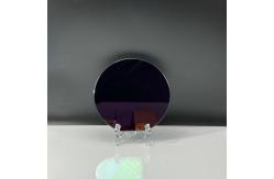
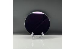
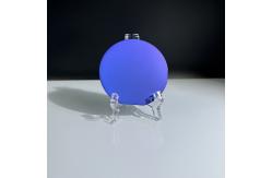
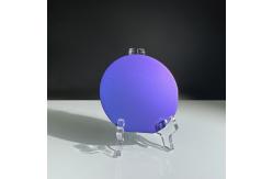
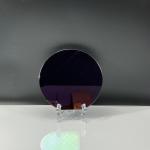
Semi Insulating GaN-On-Silicon Wafer Free Standing Gallium Nitride Substrates
|
|
Gallium Nitride Substrates GaN Wafers GaN-On-Silicon Free-Standing Substrate Semi-insulting
We can offer 2 to 8-inch gallium nitride (GaN) single crystal substrate or epitaxial sheet, and sapphire/silicon-based 2 to 8-inch GaN epitaxial sheets are available.
The rapid development of the first and second generation semiconductor materials represented by silicon (Si) and gallium arsenide (GaAs) has promoted the rapid development of microelectronics and optoelectronics technology. However, due to the limited properties of the material, most of the devices made of these semiconductor materials can only work in the environment below 200 ° C, which can not meet the requirements of modern electronic technology for high temperature, high frequency, high pressure and anti-radiation devices.
Gallium nitride (GaN), like silicon carbide (SiC) materials, belongs to the third generation of semiconductor materials with wide band gap width, with large band gap width, high thermal conductivity, high electron saturation migration rate, and high breakdown electric field outstanding characteristics. GaN devices have a wide range of application prospects in high frequency, high speed and high power demand fields such as LED energy-saving lighting, laser projection display, new energy vehicles, smart grid, 5G communication.
The third-generation semiconductor materials mainly include SiC, GaN, diamond, etc., because its band gap width (Eg) is greater than or equal to 2.3 electron volts (eV), also known as wide band gap semiconductor materials. Compared with the first and second generation semiconductor materials, the third generation semiconductor materials have the advantages of high thermal conductivity, high breakdown electric field, high saturated electron migration rate, and high bonding energy, which can meet the new requirements of modern electronic technology for high temperature, high power, high pressure, high frequency and radiation resistance and other harsh conditions. It has important application prospects in the fields of national defense, aviation, aerospace, oil exploration, optical storage, etc., and can reduce energy loss by more than 50% in many strategic industries such as broadband communications, solar energy, automobile manufacturing, semiconductor lighting, and smart grid, and can reduce equipment volume by more than 75%, which is of milestone significance for the development of human science and technology.
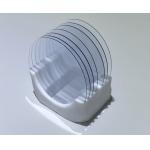
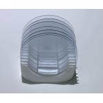
*Can be customized according to customer requirements, different structure of silicon, sapphire, SiC based GaN epitaxial sheet
Our other related products wafers About our company SHANGHAI FAMOUS TRADE CO.,LTD. locates in the city of Shanghai,
Which is the best city of China, and our factory is founded in Wuxi
city in 2014. We specialize in processing a varity of materials into wafers,
substrates and custiomized optical glass parts.components widely
used in electronics, optics, optoelectronics and many other fields.
We also have been working closely with many domestic and oversea
universities, research institutions and companies, provide
customized products and services for their R&D projects. It's our vision to maintaining a good relationship of cooperation
with our all customers by our good reputatiaons. |
|||||||||||||||||||||||||||||||||||||||||||||||||||||||||||||||||
| Product Tags: Semi Insulating GaN-On-Silicon Wafer Free Standing Gallium Nitride Substrates 350um GaN-On-Silicon Wafer | |||||||||||||||||||||||||||||||||||||||||||||||||||||||||||||||||
|
Semi Insulating GaN-On-Silicon Wafer Free Standing Gallium Nitride Substrates |
|
1inch 2inch Beta Coefficient Ga2O3 Gallium Oxide Wafer Substrate Dsp Ssp |
|
Beta Coefficient-Ga2O3 Gallium Oxide Wafer Doped Mg Fe3+ Square Substrate Dsp Ssp |

|
Large Thickness SiO2 Thermal Oxide On Silicon Wafers For Optical Communication System |
|
Y-42 Degree 4inch Lithium Tantalate LiTaO3 LiNbO3 Lithium Niobate Crystal Raw Unprocessed Ingots |

|
Single Crystal InP Indium Phosphide Wafers 350 - 650um Thickness |