
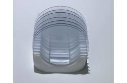
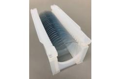
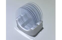
Beta Coefficient-Ga2O3 Gallium Oxide Wafer Doped Mg Fe3+ Square Substrate Dsp Ssp
|
|
Gallium Oxide Epiwafers Beta Coefficient-Ga2O3 Gallium Oxide Wafer Doped Mg Fe3+ Square Substrate Dsp Ssp
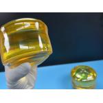
Properties of Ga2O3 β-Ga2O3 is a gallium oxide compound, which is a wide band gap semiconductor material. Its crystal structure belongs to the hexagonal crystal system, with high electron mobility and large band width, so it has a wide application prospect. Here are some details about β-Ga2O3: Physical properties: Crystal structure: hexagonal crystal system Density: 5.88 g/cm³ Lattice constant: a = 0.121 nm, c = 0.499 nm Melting point: 1725 °C Refractive index: 1.9-2.5 Transparent wavelength range: 0.23-6.0μm Electrical properties: Band width: 4.8eV Electron mobility: 200-600 cm²/Vs Leakage rate: 10^ -5-10 ^-10 A/cm² REDOX potential: 2.5V vs. NHE The Application of Ga2O3
Because of its wide band gap and high electron mobility, β-Ga2O3 has a wide application prospect in power electronics, photoelectronics, solar cells and other fields. Specific applications include:
Ultraviolet detectors and lasers High power MOSFETs and Schottky diodes High temperature sensor and potential sensor Solar cells and LED materials β-Ga2O3 still faces some challenges in preparation and application, such as crystal growth, impurity control, device fabrication, etc. However, with the continuous development of technology, the application prospect of β-Ga2O3 is still very broad.
|
|||||||||||||||||||||||||||||||||||||||||||||||||||||||||||||||||||||||||||||||||||||||||||||||||||||||||||||||||||||||||||||||||||||||||||||||||||||||||||||||||||||||||||||||||||||||||||||||||||||||||
| Product Tags: Beta Coefficient Ga2O3 Gallium Oxide Wafer Dsp Gallium Oxide Semiconductor Substrate Square Gallium Oxide Wafer | |||||||||||||||||||||||||||||||||||||||||||||||||||||||||||||||||||||||||||||||||||||||||||||||||||||||||||||||||||||||||||||||||||||||||||||||||||||||||||||||||||||||||||||||||||||||||||||||||||||||||
|
Semi Insulating GaN-On-Silicon Wafer Free Standing Gallium Nitride Substrates |
|
1inch 2inch Beta Coefficient Ga2O3 Gallium Oxide Wafer Substrate Dsp Ssp |
|
Beta Coefficient-Ga2O3 Gallium Oxide Wafer Doped Mg Fe3+ Square Substrate Dsp Ssp |

|
Large Thickness SiO2 Thermal Oxide On Silicon Wafers For Optical Communication System |
|
Y-42 Degree 4inch Lithium Tantalate LiTaO3 LiNbO3 Lithium Niobate Crystal Raw Unprocessed Ingots |

|
Single Crystal InP Indium Phosphide Wafers 350 - 650um Thickness |