
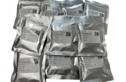
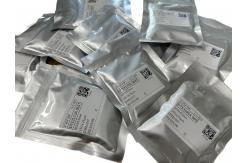
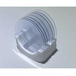
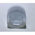
Single Crystal InP Indium Phosphide Wafers 350 - 650um Thickness
|
Detailed Product Description
|
2inch InP wafers 3inch 4inch N/P TYPE InP Semiconductor Substrate Wafers Doped S+/ Zn+ /Fe + Indium Phosphide Based Epitaxial Wafer Single Crystal Indium Phosphide Wafers InP wafer 2 inch/3 inch/4 inch 350-650 um InP Crystal Wafer Dummy Prime Semiconductor Substrate
Shanghai Xinkehui New Materials Co. Ltd. We specialize in processing a varity of materials into wafers,
substrates and custiomized optical glass parts.components widely
used in electronics, optics, electronics and many other fields. We
also have been working closely with many domestic and oversea
universities, research institutions and companies, provide
customized products and services for their R&D projects. It's
our vision to maintaining a good relationship of cooperation with
our all customers by our good reputatiaons.
It has the advantages of high electronic limit drift speed, good
radiation resistance, and good heat conduction. Suitable for Features of Inp Wafer1. The crystal is grown by liquid-sealed straight-drawing
technology (LEC), with mature technology and stable electrical performance. 2. using X-ray directional instrument for precise orientation, the crystal orientation deviation is only ±0.5° 3. the wafer is polished by chemical mechanical polishing (CMP) technology, with surface roughness <0.5nm 4. to achieve the "open box ready to use" requirements 5. according to user requirements, special specifications product processing
---FAQ – Q: Are you a trading company or manufacturer?A: zmkj is a trading company but has a sapphire manufacturer |
||||||||||||||||||||||||||||||||||||||||||||||||||||||||||
| Product Tags: Single Crystal Indium Phosphide Wafers 650um Indium Phosphide Wafers InP Semiconductor Substrate Wafers |
Related Products
|
Semi Insulating GaN-On-Silicon Wafer Free Standing Gallium Nitride Substrates |
|
1inch 2inch Beta Coefficient Ga2O3 Gallium Oxide Wafer Substrate Dsp Ssp |
|
Beta Coefficient-Ga2O3 Gallium Oxide Wafer Doped Mg Fe3+ Square Substrate Dsp Ssp |

|
Large Thickness SiO2 Thermal Oxide On Silicon Wafers For Optical Communication System |
|
Y-42 Degree 4inch Lithium Tantalate LiTaO3 LiNbO3 Lithium Niobate Crystal Raw Unprocessed Ingots |

|
Single Crystal InP Indium Phosphide Wafers 350 - 650um Thickness |
Email to this supplier