
1 - 10 of 29
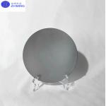
650um indium phosphide wafers
Selling leads

|
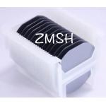
.../3 inch/4 inch 350-650 um InP Crystal Wafer Dummy Prime Semiconductor Substrate Shanghai Xinkehui New Materials Co. Ltd. We specialize in ...
2025-07-21 00:12:06
|
|
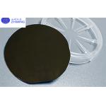
2inch/3inch/4inch S/Fe/Zn doped InP Indium Phosphide Single Crystal Wafer Indium phosphide (InP) is an important compound semiconductor material with ...
2025-05-06 20:44:34
|
|
3inch InP Indium Phosphide Substrate N-Type Semiconductor VGF growth method 000 001 orientation Product abstract Our InP (Indium Phosphide) products ...
2025-05-06 20:45:10
|
|
*, *::before, *::after {box-sizing: border-box;}* {margin: 0;}html, body {height: 100%;}body {line-height: 1.5;-webkit-font-smoothing: antialiased;...
2025-05-06 20:45:37
|
|
...wafers 3inch 4inch N/P TYPE InP Semiconductor Substrate Wafers Doped S+/ Zn+ /Fe + growth (modified VFG method) is used to pull a single crystal ...
2025-05-06 20:44:36
|

|
... innovation. Crafted from pristine indium phosphide, a binary semiconductor renowned for its superior electron velocity, our wafer offers ...
2025-05-06 20:45:10
|
|
...)) Epiwafer InP substrate dia 2 3 4 6 inch thickness:350-650um InGaAs doping FP(Fabry-Perot)) Epiwafer InP substrate's abstract Fabry-Perot (FP) ...
2025-05-06 20:45:36
|
|
...Indium Phosphide) wafers are renowned for their low defect density and high performance, widely used in optoelectronics and microelectronics. These ...
2025-05-06 20:44:24
|
|
...Indium Phosphide) semiconductor wafers, renowned for their exceptional electronic and optoelectronic properties, have found extensive applications ...
2025-05-06 20:44:23
|
|
...wafer for FP laser diode N-InP substrate FP Epiwafer's Overview Our N-InP Substrate FP Epiwafer is a high-performance epitaxial wafer designed for ...
2025-05-06 20:45:35
|