
11 - 20 of 29
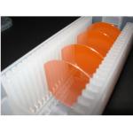
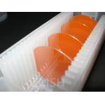
650um indium phosphide wafers
Selling leads
|
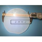
...phosphide (GaP) crystals crystal substrate,GaP wafer ZMKJ can provides 2inch GaP wafer – gallium Phosphide which are grown by LEC(Liquid Encapsulat...
2025-05-06 20:44:33
|
|
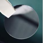
GaP Wafer, Gallium Phosphide single crystal Orientation (111)A 0°±0.2 Solar Cells Product Description: Gallium Phosphide GaP, an important semiconduct...
2025-05-06 20:45:06
|
|
2inch /3inch 4inch /5inch C-axis/ a-axis/ r-axis/ m-axis 6"/6inch dia150mm C-plane Sapphire SSP/DSP wafers with 650um/1000um Thickness About synthetic ...
2025-05-06 20:38:39
|
|
...Wafer Crystal Substrates N-Type For MBE 99.9999% Monocrystalline Introduce of InAs substrate Indium InAs or indium mono-arsenide is a semiconductor ...
2025-05-06 20:44:58
|
|
...Wafer DSP Notch High Precision 8inch/6inch/5inch/ 2inch /3inch 4inch /5inch C-axis/ a-axis/ r-axis/ m-axis 6"/6inch dia150mm C-plane Sapphire SSP...
2025-05-06 20:39:17
|
|
... growth 430um SSP DSP About synthetic sapphire crystal Due to the less mismatched lattice and stable chemical and physical properties, sapphire...
2025-07-26 00:07:39
|
|
... Substrate Indium Arsenide InAs wafer Application Indium Arsenide (InAs) single crystal semiconductor substrates are materials with unique ...
2025-07-26 00:07:38
|
|
.../ 159mm 6inch Al2O3 DSP Sapphire wafer TTV<3um for carrier plates /8inch/6inch/5inch/ 2inch /3inch 4inch /5inch C-axis/ a-axis/ r-axis/ m-axis 6"...
2025-05-06 20:40:22
|
|
... Carrier wafers for SOS GaAs epitaxy About synthetic sapphire crystal The Kyropoulos process (KY process) for sapphire crystal growth is currently ...
2025-05-06 20:38:48
|
|
...4inch /5inch C-axis/ a-axis/ r-axis/ m-axis 6"/6inch dia150mm C-plane Sapphire SSP/DSP wafers with 650um/1000um Thicknessdiameter300mm 12inch Al2O3 ...
2025-05-06 20:40:26
|