
2 Inch Gallium Phosphide Crystal Substrate GaP Wafer 0.3 Thickness Lapped Surface
|
|
2-6 inch Gallium phosphide (GaP) crystals crystal substrate,GaP wafer
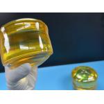
ZMKJ can provides 2inch GaP wafer – gallium Phosphide which are grown by LEC(Liquid Encapsulated Czochralski) as epi-ready or mechanical grade with n type, p type or semi-insulating in different orientation(111)or(100). Gallium phosphide (GaP), a phosphide of gallium, is a compound semiconductor material with an indirect band gap of 2.26eV(300K). The polycrystalline material has the appearance of pale orange pieces. Undoped single crystal wafers appear clear orange, but strongly doped wafers appear darker due to free-carrier absorption. It is odorless and insoluble in water.Sulfur or tellurium are used as dopants to produce n-type semiconductors. Zinc is used as a dopant for the p-type semiconductor.Gallium phosphide has applications in optical systems. Its refractive index is between 4.30 at 262 nm (UV), 3.45 at 550 nm (green) and 3.19 at 840 nm (IR).
high quality single crystal GaP wafer ( Gallium phosphide ) to electronic and optoelectronic industry in diameter up to 2 inch . Gallium phosphide ( GaP ) crystal is an orange-yellow semi-translucent material formed by two elements , GaP wafer is an important semiconductor material which have unique electrical properties as other III-V compound materials and is widely used as red , yellow , and green LED ( light-emitting diodes ) . We have as-cut single crystal GaP wafer for your LPE application , and also provide epi ready grade GaP wafer for your MOCVD & MBE epitaxial application . Please contact us for more product information .
Electrical and Doping Specification
Product Specification
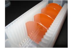
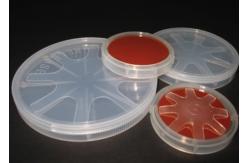
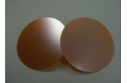
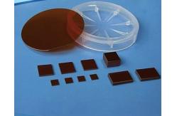
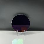
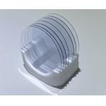
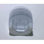
Sample pictures
OUR RELATED Products
InP Wafer ZnO wafers sic wafers customzied/ standard sapphire wafers
FAQ: Q: What's the delivery time? A: (1) For the standard products For inventory: the delivery is 5 workdays after you place the order. For customized products: the delivery is 2 or 3 weeks after you place the order. (2) For the special-shaped products, the delivery is 4 workweeks after you place the order. Q: What's your MOQ? A: (1) For inventory, the MOQ is 3pcs. (2) For customized products, the MOQ is 10-20pcs up.
|
||||||||||||||||||||||||||||||||||||||||||||||||||||||||||||||||||
| Product Tags: wafer substrate semiconductor wafer | ||||||||||||||||||||||||||||||||||||||||||||||||||||||||||||||||||
|
Semi Insulating GaN-On-Silicon Wafer Free Standing Gallium Nitride Substrates |
|
1inch 2inch Beta Coefficient Ga2O3 Gallium Oxide Wafer Substrate Dsp Ssp |
|
Beta Coefficient-Ga2O3 Gallium Oxide Wafer Doped Mg Fe3+ Square Substrate Dsp Ssp |

|
Large Thickness SiO2 Thermal Oxide On Silicon Wafers For Optical Communication System |
|
Y-42 Degree 4inch Lithium Tantalate LiTaO3 LiNbO3 Lithium Niobate Crystal Raw Unprocessed Ingots |

|
Single Crystal InP Indium Phosphide Wafers 350 - 650um Thickness |