
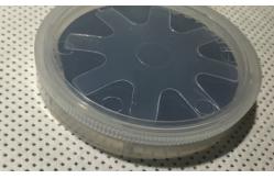
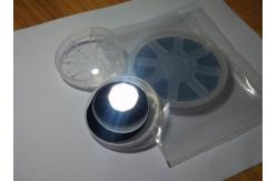
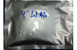
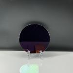
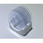
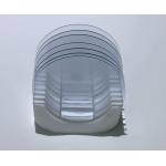
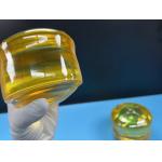
Thick 650um 4 Inch Single Crystal InP Semiconductor Substrate
|
|
2inch InP wafers 3inch 4inch N/P TYPE InP Semiconductor Substrate Wafers Doped S+/ Zn+ /Fe +
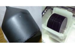
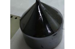
growth (modified VFG method) is used to pull a single crystal through a boric oxide liquid encapsulant starting from a seed. The dopant (Fe, S, Sn or Zn)is added to the crucible along with the
polycrystal. High pressure is applied inside the chamber to prevent
decomposition of the Indium Phosphide.he company has developed a process to yield fully stoechiometric, high purity
and low dislocation density inP single crystal. modeling of thermal growth conditions. tCZ is a cost-effective mature technology with high quality reproducibility from boule to boule.
Applications:
Features:
---FAQ – Q: Are you trading company or manufacturer ?A: zmkj is a trading company but have a sapphire manufacturer |
||||||||||||||||||||||||||||||||||||||||
| Product Tags: InP Semiconductor Substrate Single Crystal Semiconductor Substrate 650um InP wafers | ||||||||||||||||||||||||||||||||||||||||
|
Semi Insulating GaN-On-Silicon Wafer Free Standing Gallium Nitride Substrates |
|
1inch 2inch Beta Coefficient Ga2O3 Gallium Oxide Wafer Substrate Dsp Ssp |
|
Beta Coefficient-Ga2O3 Gallium Oxide Wafer Doped Mg Fe3+ Square Substrate Dsp Ssp |

|
Large Thickness SiO2 Thermal Oxide On Silicon Wafers For Optical Communication System |
|
Y-42 Degree 4inch Lithium Tantalate LiTaO3 LiNbO3 Lithium Niobate Crystal Raw Unprocessed Ingots |

|
Single Crystal InP Indium Phosphide Wafers 350 - 650um Thickness |