
1 - 10 of 24
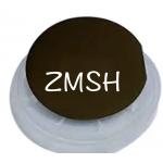
650um inp wafers
Selling leads
|
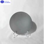
...InP (Indium Phosphide) semiconductor wafers, renowned for their exceptional electronic and optoelectronic properties, have found extensive ...
2025-05-06 20:44:23
|
|
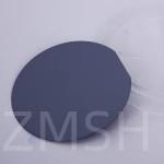
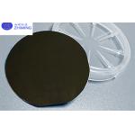
...InP (Indium Phosphide) wafers are renowned for their low defect density and high performance, widely used in optoelectronics and microelectronics. ...
2025-05-06 20:44:24
|

|
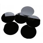
... innovation. Crafted from pristine indium phosphide, a binary semiconductor renowned for its superior electron velocity, our wafer offers ...
2025-05-06 20:45:10
|
|
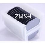
InP wafer 2inch 3inch 4inch VGF P type N type Depant Zn S Fe Undoped Prime Grade Testing Grade *, *::before, *::after {box-...
2025-05-06 20:45:30
|

|
.../3 inch/4 inch 350-650 um InP Crystal Wafer Dummy Prime Semiconductor Substrate Shanghai Xinkehui New Materials Co. Ltd. We specialize in ...
2025-07-30 00:08:00
|
|
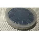
2inch InP wafers 3inch 4inch N/P TYPE InP Semiconductor Substrate Wafers Doped S+/ Zn+ /Fe + growth (modified VFG method) is used to pull a single ...
2025-05-06 20:44:36
|
|
...InP substrate dia 2 3 4 6 inch thickness:350-650um InGaAs doping FP(Fabry-Perot)) Epiwafer InP substrate's abstract Fabry-Perot (FP) Epiwafer on ...
2025-05-06 20:45:36
|
|
...InP substrate bandwidth 02:2.5G wavelength 1270nm epi wafer for FP laser diode N-InP substrate FP Epiwafer's Overview Our N-InP Substrate FP ...
2025-05-06 20:45:35
|
|
2inch InP wafers 3inch 4inch N/P TYPE InP Semiconductor Substrate Wafers Doped S+/ Zn+ /Fe + growth (modified VFG method) is used to pull a single ...
2025-05-06 20:44:37
|
|
InP DFB Epiwafer wavelength 1390nm InP substrate 2 4 6 inch for 2.5~25G DFB laser diode InP DFB Epiwafer InP substrate's brief InP DFB Epiwafers ...
2025-05-06 20:45:38
|