
101 - 110 of 311
inp semiconductor substrate wafers
Selling leads
|
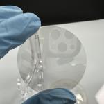
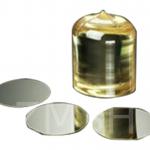
...substrate wafers. Our wafers are optimal for electronic devices with high power and high frequency, as well as for light emitting diodes (LED). The ...
2025-07-21 00:12:06
|
|
...substrates AlN Wafer Characteristic III-Nitride(GaN,AlN,InN) 2inch AlN template on sapphire or sic substrates, HVPE Gallium Nitride wafer,AlN ...
2025-05-06 20:44:29
|
|
dia50.8mm 2inch 1inch AlN substrate/AlN single crystal wafers 10x10mm or diameter 10mm dia25.4mm dia30mm, dia45mm, dia50.8mm AlN substrate AlN single ...
2025-05-06 20:44:42
|
|
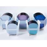
2inch 3inch 4inch LNOI LiNbO3 Wafer Lithium Niobate Thin Films Layer On Silicon Substrate LNOI wafer preparation process is shown below, including the ...
2025-05-06 20:44:59
|
|
2inch 4inch LiTaO3 Wafer Substrate Double or Single Polished Z-cut X-cut Y-cut Saw grade Description of LiTaO3 Wafer: Lithium tantalate (LiTaO3) has a ...
2025-05-06 20:45:49
|
|
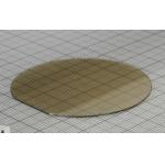
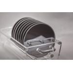
...Wafer CZ orientation111 Resistivity: 1-10 (ohm.cm) single side or double side polish Product abstract Our Si wafer offers high purity and ...
2025-05-06 20:45:12
|
|
...Wafer Thin Films Layer On Silicon Substrate Lithium niobate (LiNbO3) crystal is an important photoelectric material, and is widely used in ...
2025-05-06 20:44:57
|
Mg Substrate Magnesium Single Crystal Hexagonal 5x5x0.5/1mm 10x10x0.5/1mm20x20x0.5/1mm Purity 99.99%
|
... and hexagonal lattice structures are becoming increasingly important in material science, particularly for applications requiring lightweight yet ...
2025-05-06 20:45:47
|
|
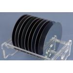
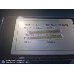
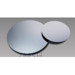
... wafers silicon carbon chips for optical About Silicon Carbide (SiC)Crystal Silicon carbide (SiC), also known as carborundum, is a semiconductor ...
2025-05-06 20:40:52
|
|
...Silicon Wafers Ultra-High Purity Optoelectronic-Grade Abstract The high-purity silicon wafer we offer undergoes precision machining and strict ...
2025-05-06 20:45:04
|