
131 - 140 of 311
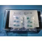
inp semiconductor substrate wafers
Selling leads
|
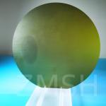
... as-cut sic wafers 6H-N/6H-Semi 4H HPSI 5*10mmt 10x10mmt 5*5mm polished Silicon Carbide sic substrate chips Wafer About Silicon Carbide (SiC...
2025-05-06 20:40:49
|
|
... Wafer Characteristic III-Nitride(GaN,AlN,InN) Gallium Nitride is one kind of wide-gap compound semiconductors. Gallium Nitride (GaN) substrate is ...
2025-05-06 20:44:18
|
|
... Wafer Characteristic III-Nitride(GaN,AlN,InN) Gallium Nitride is one kind of wide-gap compound semiconductors. Gallium Nitride (GaN) substrate is ...
2025-05-06 20:44:18
|

|
SapphiLarge Thickness Thermal Oxide (SiO2) On Silicon Wafers For Optical Communication System Generally, the oxide layer thickness of silicon wafers ...
2025-07-21 00:12:06
|
|
... optical applications, particularly for Gigabit Ethernet and digital data link communication. Built on a 6-inch wafer, it features a high ...
2025-05-06 20:45:39
|
|
... single-crystal SiC on polycrystalline SiC composite substrate is a new type of semiconductor substrate structure. Its core lies in bonding or ...
2025-05-13 05:30:20
|
|
...LED, mocvd Gallium Nitride wafer 10x10mm,5x5mm, 10x5mm GaN wafer,Non-Polar Freestanding GaN Substrates(a-plane and m-plane) 4inch 2inch free...
2025-05-06 20:44:19
|
|
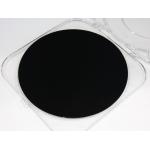
... containing silicon and carbon with chemical formula SiC. SiC is used in semiconductor electronics devices that operate at high temperatures or ...
2025-05-06 20:40:48
|
|
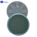
Abstract The 4-H Semi-Insulating SiC substrate is a high-performance semiconductor material with a wide range of applications. It derives its name ...
2025-07-21 00:12:06
|
|
GaP Wafer, Gallium Phosphide single crystal Orientation (111)A 0°±0.2 Solar Cells Product Description: Gallium Phosphide GaP, an important semiconduct...
2025-05-06 20:45:06
|