
N-GaAs Substrate 6inch 350um Thickness For VCSEL Use OptiWave VCSEL EpiWafer
|
|
N-GaAs substrate 6inch 350um thickness for VCSEL use OptiWave VCSEL epiWafer
VCSEL epiWafer N-GaAs substrate' s abstract
The VCSEL epiWafer on N-GaAs substrate is designed for high-performance optical applications, particularly for Gigabit Ethernet and digital data link communication. Built on a 6-inch wafer, it features a high uniformity laser array and supports center optical wavelengths of 850 nm and 940 nm. The structure is available in either oxide-confined or proton implant VCSEL configurations, ensuring flexibility in design and performance. The wafer is optimized for applications requiring low dependence on electrical and optical characteristics over temperature, making it ideal for use in laser mice, optical communication, and other temperature-sensitive environments.
VCSEL epiWafer N-GaAs substrate's structure
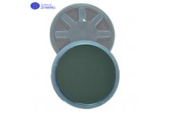
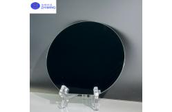
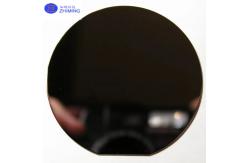
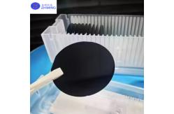
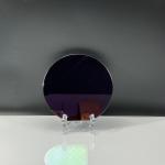
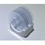
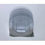
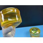
VCSEL epiWafer N-GaAs substrate' s photo
VCSEL epiWafer N-GaAs substrate' s datasheetZMSH VCSEL EPIWAFER.pdf
VCSEL epiWafer N-GaAs substrate' s properties
The VCSEL epiWafer on N-GaAs substrate has several key properties that make it suitable for high-performance optical applications:
N-GaAs Substrate:
Wavelength Tunability:
High Uniformity Laser Array:
Oxide-Confined or Proton Implant:
Thermal Stability:
High Power and Speed:
Scalability:
These properties make the VCSEL epiWafer on N-GaAs substrate ideal for applications requiring high efficiency, temperature stability, and reliable performance. |
| Product Tags: 350um VCSEL N-GaAs substrate 350um N-GaAs substrate 6inch N-GaAs substrate |
|
Semi Insulating GaN-On-Silicon Wafer Free Standing Gallium Nitride Substrates |
|
1inch 2inch Beta Coefficient Ga2O3 Gallium Oxide Wafer Substrate Dsp Ssp |
|
Beta Coefficient-Ga2O3 Gallium Oxide Wafer Doped Mg Fe3+ Square Substrate Dsp Ssp |

|
Large Thickness SiO2 Thermal Oxide On Silicon Wafers For Optical Communication System |
|
Y-42 Degree 4inch Lithium Tantalate LiTaO3 LiNbO3 Lithium Niobate Crystal Raw Unprocessed Ingots |

|
Single Crystal InP Indium Phosphide Wafers 350 - 650um Thickness |