
141 - 150 of 311
inp semiconductor substrate wafers
Selling leads
|
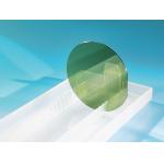
ZnTe: ZnTe wafer, ZnTe crystal Type N, Type P, Custom Sizes and Specifications Available Abstract of ZnTe Zinc telluride (ZnTe) is a direct bandgap ...
2025-05-06 20:45:56
|
|
...substrates wafersS/ Customzied as-cut sic wafers About Silicon Carbide (SiC)Crystal Silicon carbide (SiC), also known as carborundum, is a ...
2025-05-06 20:40:40
|
|
...substrates wafersS/ Customzied as-cut sic wafers About Silicon Carbide (SiC)Crystal Silicon carbide (SiC), also known as carborundum, is a ...
2025-05-06 20:40:40
|
|
...0001) orientation 8inch diameter 200mm with notch DSP Sapphire Substrate wafers thickness 1.15mm C-a Sapphire application Application Sapphire ...
2025-05-06 20:40:27
|
|
... on the market for 2 inch and 3 inch Research grade SiC substrate wafers. SiC substrate wafers have a variety of applications in electronic device ...
2025-07-21 00:12:06
|
|
... semiconductor applications, featuring a 300mm diameter, 750±25µm thickness, and a 4H-N type crystal orientation with a polytype of 4H-SiC. The ...
2025-05-06 20:41:55
|
|
LiTaO3 Wafer Lithium Tantalate Electro-Optic Nonlinear Optical Piezoelectric Customization Introduce of LiTaO3 Wafer Lithium tantalate is an excellent ...
2025-06-23 17:12:59
|
|
LNOI Wafer 2/3/4/6/8 Inch (Si/LiNbO₃, Customizable) photonic devices Introduce of LNOI Wafer LiNbO3 Crystals is widely used as frequency doublers for ...
2025-06-23 17:12:58
|
|
...Substrate Silicon carbide subatrte 4H/6H-P 3C-N 5×5 10×10mm P grade R grade D grade 4H/6H-P SiC Substrate 5×5 10×10mm's abstratct The 4H/6H-P ...
2025-05-06 20:41:41
|

|
...substrates template,GaN wafer for LeD,semiconducting Gallium Nitride Wafer for ld,GaN template, mocvd GaN Wafer,Free-standing GaN Substrates by ...
2025-05-06 20:44:12
|