
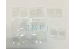
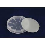
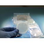
5x5/10x10 Mm Gallium Nitride Wafer HVPE Free Standing Chip Template Industrial
|

|
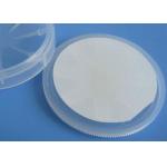
2inch GaN substrates template,GaN wafer for LeD,semiconducting Gallium Nitride Wafer for ld,GaN template, mocvd GaN Wafer,Free-standing GaN Substrates by Customized size,small size GaN wafer for LED, mocvd Gallium Nitride wafer 10x10mm,5x5mm, 10x5mm GaN wafer,Non-Polar Freestanding GaN Substrates(a-plane and m-plane)
GaN Wafer Characteristic
Application GaN can be used in many areas such as LED display, High-energy
Detection and Imaging,
Specifications:
Q&A
Q:What is a GaN wafer? A:A GaN wafer (gallium nitride wafer) is a thin, flat substrate made from gallium nitride, a wide-bandgap semiconductor material that is widely used in high-performance electronics. GaN wafers are the foundation for manufacturing electronic devices, particularly for applications requiring high power, high frequency, and high efficiency. This material is especially important in industries such as power electronics, telecommunications, and LED lighting.
Q:Why is GaN better than silicon? A:GaN (gallium nitride) is better than silicon in many high-performance applications due to its wide bandgap (3.4 eV compared to silicon's 1.1 eV), enabling GaN devices to operate at higher voltages, temperatures, and frequencies. GaN's high efficiency leads to lower heat generation and reduced energy loss, making it ideal for power electronics, fast-charging systems, and high-frequency applications. Additionally, GaN has better thermal conductivity, allowing devices to run more efficiently in demanding conditions. As a result, GaN-based devices are more compact, energy-efficient, and reliable than their silicon counterparts.
Key words:#GaN #GalliumNitride #PowerElectronics #HighPerformance #Efficiency #LED #LaserProjection #EnergyEfficientLighting #HighFrequencyDevices #NonPolarGaN #FreestandingGaN #GaNSubstrates #MOCVD |
|||||||||||||||||||||||||||||||||||||||||||||||||||||||||||||||||||||||
| Product Tags: gan wafer gallium phosphide wafers | |||||||||||||||||||||||||||||||||||||||||||||||||||||||||||||||||||||||
|
2Inch 4inch free-standing GaN Gallium Nitride Wafer |
|
5um Thickness AlN Aluminum Nitride Template 430um Sapphire 350um Sic Substrates |
|
2 4 Inch 4-5 Um III Gallium Nitride Wafer 0.43 Mm Sapphire Sic Substrates |
|
III - Nitride 2 INCH Free Standing GaN Wafer For Laser Projection Display Power Device |
|
2inch 4inch GaN-based Blue Green LED Grown On Flat Or PPS Sapphire MOCVD DSP SSP |
|
8inch GaN-on-Si Epitaxy Wafer 110 111 110 N Type P Type Customization Semiconductor RF LED |