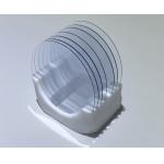
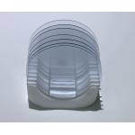
LNOI Wafer 2/3/4/6/8 Inch (Si/LiNbO₃, Customizable) photonic
devices
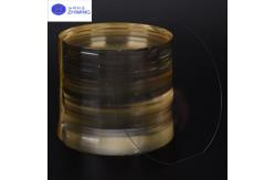
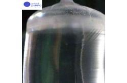
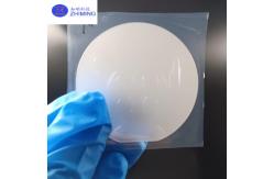
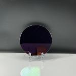
Introduce of LNOI Wafer
LiNbO3 Crystals is widely used as frequency doublers for wavelength
> 1um and optical parametric oscillators (OPOs) pumped at
1064 nm as well as quasi-phase-matched (QPM) devices. Due to its
large Elector-Optic (E-O) and Acousto-Optic (A-O) coefficients,
LiNbO3 crystal is the most commonly used material for Pockel Cells,
Q-switches and phase modulators, waveguide substrate, and surface
acoustic wave (SAW) wafers, etc.
Our abundance experience at growing and mass production for Optical
grade Lithium Niobate on both boule and wafers. We are equipped
with advanced facilities at Crystal growing, slicing, wafer
lapping, polishing and checking, all finished products are passed
at Testing of curie Temp and QC inspection. All the wafers are
under strict quality control and inspected. And also under the
strict surface cleaning and flatness control as well.
Specification of LNOI Wafer
| Material | Optical Grade LiNbO3 wafers |
| Curie Temp | 1142±0.7℃ |
| Cutting Angle | X/Y/Z etc |
| Diameter/size | 2”/3”/4”/6"/8” |
| Tol(±) | <0.20 mm ±0.005mm |
| Thickness | 0.18~0.5mm or more |
| Primary Flat | 16mm/22mm/32mm |
| TTV | <3μm |
| Bow | -30<bow<30 |
| Warp | <40μm |
| Orientation Flat | All available |
| Surface Type | Single Side Polished(SSP)/Double Sides Polished(DSP) |
| Polished side Ra | <0.5nm |
| S/D | 20/10 |
| Edge Criteria | R=0.2mm C-type or Bullnose |
| Quality | Free of crack(bubbles and inclusions) |
| Optical doped | Mg/Fe/Zn/MgO etc for optical grade LN< wafers per requested |
| Wafer Surface Criteria | Refractive index | No=2.2878/Ne=2.2033 @632nm wavelength/prism coupler method. |
| Contamination, | None |
| Particles c>0.3μ m | <=30 |
| Scratch,Chipping | None |
| Defect | No edge cracks,scratches,saw marks,stains |
| Packaging | Qty/Wafer box | 25pcs per box |
Properties of LNOI Wafer
The fabrication of Lithium Niobate on Insulator (LNOI) wafers
involves a sophisticated series of steps that combine material
science and advanced fabrication techniques. The process aims to
create a thin, high-quality lithium niobate (LiNbO₃) film bonded to
an insulating substrate, such as silicon or lithium niobate itself.
The following is a detailed explanation of the process:
Step 1: Ion Implantation
The first step in the production of LNOI wafers involves ion
implantation. A bulk lithium niobate crystal is subjected to
high-energy helium (He) ions injected into its surface. The ion
implantation machine accelerates the helium ions, which penetrate
the lithium niobate crystal to a specific depth.
The energy of the helium ions is carefully controlled to achieve
the desired depth in the crystal. As the ions travel through the
crystal, they interact with the lattice structure of the material,
causing atomic disruptions that lead to the formation of a weakened
plane, known as the "implantation layer." This layer will
eventually allow the crystal to be cleaved into two distinct
layers, where the top layer (referred to as Layer A) becomes the
thin lithium niobate film needed for LNOI.
The thickness of this thin film is directly influenced by the
implantation depth, which is controlled by the energy of the helium
ions. The ions form a Gaussian distribution at the interface, which
is crucial for ensuring uniformity in the final film.
Step 2: Substrate Preparation
Once the ion implantation process is complete, the next step is to
prepare the substrate that will support the thin lithium niobate
film. For LNOI wafers, common substrate materials include silicon
(Si) or lithium niobate (LN) itself. The substrate must provide
mechanical support for the thin film and ensure long-term stability
during the subsequent processing steps.
To prepare the substrate, a SiO₂ (silicon dioxide) insulating layer
is typically deposited onto the surface of the silicon substrate
using techniques such as thermal oxidation or PECVD
(Plasma-Enhanced Chemical Vapor Deposition). This layer serves as
the insulating medium between the lithium niobate film and the
silicon substrate. In some cases, if the SiO₂ layer is not
sufficiently smooth, a Chemical Mechanical Polishing (CMP) process
is applied to ensure that the surface is uniform and ready for the
bonding process.
Step 3: Thin-Film Bonding
After preparing the substrate, the next step is to bond the thin
lithium niobate film (Layer A) to the substrate. The lithium
niobate crystal, after ion implantation, is flipped 180 degrees and
placed onto the prepared substrate. The bonding process is
typically carried out using a wafer bonding technique.
In wafer bonding, both the lithium niobate crystal and the
substrate are subjected to high pressure and temperature, which
causes the two surfaces to adhere strongly. The direct bonding
process usually does not require any adhesive materials, and the
surfaces are bonded at the molecular level. For research purposes,
benzocyclobutene (BCB) may be used as an intermediate bonding
material to provide additional support, though it is typically not
used in commercial production due to its limited long-term
stability.
Step 4: Annealing and Layer Splitting
After the bonding process, the bonded wafer undergoes an annealing
treatment. Annealing is crucial for improving the bond strength
between the lithium niobate layer and the substrate, as well as for
repairing any damage caused by the ion implantation process.
During annealing, the bonded wafer is heated to a specific
temperature and maintained at that temperature for a certain
duration. This process not only strengthens the interfacial bonds
but also induces the formation of microbubbles in the ion-implanted
layer. These bubbles gradually cause the lithium niobate layer
(Layer A) to separate from the original bulk lithium niobate
crystal (Layer B).
Once the separation occurs, mechanical tools are used to cleave the
two layers apart, leaving behind a thin, high-quality lithium
niobate film (Layer A) on the substrate. The temperature is
gradually reduced to room temperature, completing the annealing and
layer separation process.
Step 5: CMP Planarization
After the separation of the lithium niobate layer, the surface of
the LNOI wafer is typically rough and uneven. To achieve the
required surface quality, the wafer undergoes a final Chemical
Mechanical Polishing (CMP) process. CMP smooths out the surface of
the wafer, removing any remaining roughness and ensuring that the
thin film is planar.
The CMP process is essential for obtaining a high-quality finish on
the wafer, which is critical for subsequent device fabrication. The
surface is polished to a very fine level, often with a roughness
(Rq) of less than 0.5 nm as measured by Atomic Force Microscopy
(AFM).
Applications of LNOI wafer
LNOI (Lithium Niobate on Insulator) wafers are utilized in a wide
range of advanced applications due to their exceptional properties,
including high nonlinear optical coefficients and strong mechanical
characteristics. In integrated optics, LNOI wafers are essential
for creating photonic devices such as modulators, waveguides, and
resonators, which are critical for manipulating light in integrated
circuits. In telecommunications, LNOI wafers are widely used in
optical modulators, which enable high-speed data transmission in
fiber-optic networks. In the field of quantum computing, LNOI
wafers play a vital role in generating entangled photon pairs,
which are fundamental for quantum key distribution (QKD) and secure
communication. Additionally, LNOI wafers are utilized in various
sensor applications, where they are used to create highly sensitive
optical and acoustic sensors for environmental monitoring, medical
diagnostics, and industrial processes. These diverse applications
make LNOI wafers a key material in the development of
next-generation technologies across multiple fields.
FAQ of LNOI Wafer
Q:What is LNOI?
A:LNOI stands for Lithium Niobate on Insulator. It refers to a type
of wafer that features a thin layer of lithium niobate (LiNbO₃)
bonded to an insulating substrate like silicon or another
insulating material. LNOI wafers retain the excellent optical,
piezoelectric, and pyroelectric properties of lithium niobate,
making them ideal for use in various photonic, telecommunications,
and quantum technologies.
Q:What are the main applications of LNOI wafers?
A:LNOI wafers are used in a variety of applications, including
integrated optics for photonic devices, optical modulators in
telecommunications, entangled photon generation in quantum
computing, and in sensors for optical and acoustic measurements in
environmental monitoring, medical diagnostics, and industrial
testing.
Q:How are LNOI wafers fabricated?
A:The fabrication of LNOI wafers involves several steps, including
ion implantation, bonding of the lithium niobate layer to a
substrate (usually silicon), annealing for separation, and chemical
mechanical polishing (CMP) to achieve a smooth, high-quality
surface. The ion implantation creates a thin, fragile layer that
can be separated from the bulk lithium niobate crystal, leaving
behind a thin, high-quality lithium niobate film on the substrate.
Related products
Lithium Niobate (LiNbO3) Crystal EO/PO Components Telecom Defense
High-Frequency SAW