
121 - 130 of 311
inp semiconductor substrate wafers
Selling leads
|
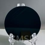
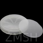
SOI Wafer Silicon-on-Insulator Wafer 4inch 5inch 6inch 8inch (100) (111) P Type N Type Description of SOI Wafer: SOI wafer refers to a thin layer of ...
2025-05-06 20:45:41
|
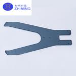
SiC Wafer Hand for Wafer Handling, Cleanroom Compatible, Corrosion Resistant, Customizable Interface
|
..., it offers excellent mechanical strength, corrosion resistance, thermal durability, and ultra-clean performance. It is ideal for handling advanced ...
2025-05-29 00:09:29
|
|
...wafer 1-5um AlN template 8inch 6inch AlGaN/GaN HEMT-on-HR Si Epiwafer GaN-on-Si Epiwafer for Micro-LED for RF application GaN Wafer Characteristic ...
2025-05-06 20:44:19
|
|
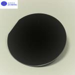
N-type SiC on Si Compound Wafer 6inch 150mm SiC type 4H-N Si type N or P N-type SiC on Si Compound Wafer abstract N-type silicon carbide (SiC) on ...
2025-05-06 20:45:18
|
|
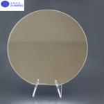
MgO Wafer (111) (100) Polished Magnesium oxide Monocrystal Semiconductor Customized *, *::before, *::after {box-sizing: border-box;}* {margin: 0;}html...
2025-05-06 20:45:34
|
|
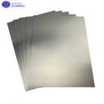
... Carbide substrates wafers. SiC substrates wafers are widely used in electronic devices with high power and high frequency. Light Emitting Diode ...
2025-07-21 00:12:06
|
|
...substrate Epitaxy 4inch 6inch 8inch for LED or Power device GaN-on-Si substrate abstract GaN-on-Si (111) substrates are essential in high...
2025-05-06 20:45:21
|
|
... used in material science and electronics research due to their versatile properties. Available in dimensions of 5x5x0.5 mm, 10x10x1 mm, and ...
2025-05-06 20:45:48
|
|
4inch 6inch 300-900 nm Lithium Niobate LiNbO3 LN Thin Films (LNOI) on silicon wafer Direction of application: · Electro-Optic Modulators · Delay Lines ...
2025-05-06 20:44:42
|
|
... the best price on the market for 2 inch and 3 inch Research grade Silicon Carbide substrate wafers, but also provides innovative solutions for ...
2025-07-21 00:12:06
|