
111 - 120 of 311
inp semiconductor substrate wafers
Selling leads
|
... technology, revolutionizing the landscape of advanced electronics. Comprising three distinct layers, this cutting-edge wafer embodies a trifecta ...
2025-05-06 20:45:07
|
|
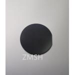
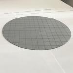
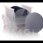
...Wafer 6inch(0001)Double Side Polished Ra≤1 nm Customization Description of 12 inch SiC wafer 4H N-type Semi-type SiC Wafer: 12 inch 6inch SiC wafer ...
2025-05-06 20:41:28
|
|
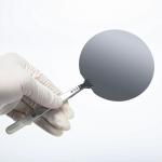
6inch 8inch 2inch 1inch FZ CZ N-type polished silicon wafer DSP SiO2 wafers Silicon oxide wafer Polished Silicon Wafer High-purity (11N) 1-12 inch ...
2025-05-06 20:44:51
|
|
6inch 8inch 2inch 1inch FZ CZ N-type polished silicon wafer DSP SiO2 wafers Silicon oxide wafer Polished Silicon Wafer High-purity (11N) 1-12 inch ...
2025-05-06 20:44:47
|
|
2inch 3inch 4inch 5inch 6inch 8inch 12inch FZ CZ N-type polished silicon wafer DSP SiO2 wafers Silicon oxide wafer 1inch 2inch 10x10mm Scanning ...
2025-05-06 20:44:47
|
|
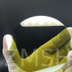
...wafer optical 1/2/3 inch SIC wafer for sale Sic Plate Silicon Wafer Flat Orientation Enterprises for Sale 4inch 6inch seed sic wafer 1.0mm ...
2025-07-21 00:12:06
|
|
...wafer optical 1/2/3 inch SIC wafer for sale Sic Plate Silicon Wafer Flat Orientation Enterprises for Sale 4inch 6inch seed sic wafer 1.0mm ...
2025-07-21 00:12:06
|
|
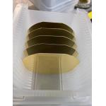
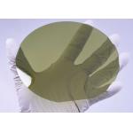
...Substrates 4H and 6H Epi-Ready SiC Substrate/Wafers (150mm, 200mm) Silicon Carbide(SiC) wafer N Type 6inch SIC Wafer 4H-N Type production grade sic ...
2025-05-06 20:41:08
|
|
...) are 3D integrated at the wafer scale. The two wafers are bonded face-to-face using a low-temperature oxide-oxide bonding technique. The Si ...
2025-05-06 20:44:26
|
|
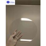
Fused Silica wafer JGS1 JGS2 BF33 8inch 12inch thickeness 750um±25um Ra ≤ 0.5nm TTV ≤ 10um Fused Silica wafer JGS1 JGS2 BF33 8inch 12inch‘s summary ...
2025-05-06 20:45:40
|