
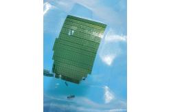
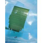
Square SiC Windows Silicon Carbide Substrate 1x1x0.5mmt SiC Lens
|
|
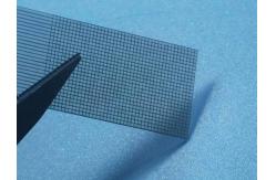
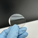
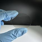
Silicon carbide wafer optical 1/2/3 inch SIC wafer for sale Sic Plate Silicon Wafer Flat Orientation Enterprises for Sale 4inch 6inch seed sic wafer 1.0mm Thickness 4h-N SIC Silicon Carbide Wafer For seed growth 6H-N/6H-Semi 4H HPSI 5*10mmt 10x10mmt 5*5mm polished Silicon Carbide sic substrate chips Wafer About Silicon Carbide (SiC)CrystalSilicon carbide (SiC), or carborundum, is a semiconductor containing silicon and carbon with the chemical formula SiC. SiC is used in semiconductor electronics devices operating at high temperatures, high voltages, or both. SiC is also one of the important LED components, it is a popular substrate for growing GaN devices, and it also serves as a heat spreader in high-power LEDs. 1. Description
High purity 4inch diameter Silicon Carbide (SiC) Substrate
Specification
SiC Applications
Silicon carbide (SiC) crystals have unique physical and electronic properties. Silicon Carbide based devices have been used for short wavelength optoelectronic, high temperature, radiation resistant applications. The high-power and high-frequency electronic devices made with SiC are superior to Si and GaAs-based devices. Below are some popular applications of SiC substrates.
Other products 8inch SiC wafer dummy grade 2inch SiC wafer
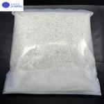
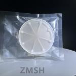
Packaging – Logistics According to the quantity and shape of the product, we will take a different packaging process! Almost by single wafer cassettes or 25pcs cassettes in the 100-grade cleaning room.
|
||||||||||||||||||||||||||||||||||||||||||||||||||||||||||||||||||||||||||||||||||||||||||||||||||||||||||||||||||||||||||||||||||||||||||||||||||||||||||||||||||||||||||||||||||||||||||||||||||||||||||||||||||||||||||||||||||||||||||||||||||||||||||||||||||||||||||||||||||||||||||||||||||||||||||||
| Product Tags: Square SiC Windows Square Silicon Carbide Substrate 4H-N Type Silicon Carbide Wafer | ||||||||||||||||||||||||||||||||||||||||||||||||||||||||||||||||||||||||||||||||||||||||||||||||||||||||||||||||||||||||||||||||||||||||||||||||||||||||||||||||||||||||||||||||||||||||||||||||||||||||||||||||||||||||||||||||||||||||||||||||||||||||||||||||||||||||||||||||||||||||||||||||||||||||||||
|
High Purity Semi-Insulating HPSI SiC Powder/99.9999% Purity Crystal Growth |
|
Semi-Insulating SiC Wafers 3inch 76.2mm 4H Type SiC For Semiconductors |
|
High Resistivity 8inch 200mm Silicon Carbide Wafer Production Grade 4H-N |
|
4H/6H Semi-Insulating Silicon Carbide Wafer For Production/Research/Dummy Grade |
|
Square SiC Windows Silicon Carbide Substrate 1x1x0.5mmt SiC Lens |
|
Semi Insulating Silicon Carbide Wafer SiC Substrate Orientation 0001 Bow/Warp ≤50um |