
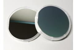
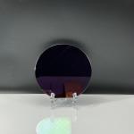
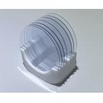
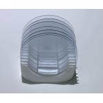
900nm 4 Inch LiNbO3 Lithium Niobate Wafer Thin Films Layer On Silicon Substrate
|
|
4inch 6inch 300-900 nm Lithium Niobate LiNbO3 LN Thin Films (LNOI) on silicon wafer Direction of application:
· Electro-Optic Modulators · Delay Lines · Electro-Optic Q Switches · X-BAR · Phase Modulator Devices · Nonlinear Optics · Ferroelectric Memory Devices
Characteristic Specification
Related Customized Thin Films
FAQ – |
|||||||||||||||||||||||||||||||||||||||||||||||||||||||||||||||||||||||||||||||||||||||||||||||||||||||||||||||||||||||||||||||
| Product Tags: LiNbO3 lithium niobate wafer 4 Inch lithium niobate wafer 900nm lithium niobate on insulator | |||||||||||||||||||||||||||||||||||||||||||||||||||||||||||||||||||||||||||||||||||||||||||||||||||||||||||||||||||||||||||||||
|
Semi Insulating GaN-On-Silicon Wafer Free Standing Gallium Nitride Substrates |
|
1inch 2inch Beta Coefficient Ga2O3 Gallium Oxide Wafer Substrate Dsp Ssp |
|
Beta Coefficient-Ga2O3 Gallium Oxide Wafer Doped Mg Fe3+ Square Substrate Dsp Ssp |

|
Large Thickness SiO2 Thermal Oxide On Silicon Wafers For Optical Communication System |
|
Y-42 Degree 4inch Lithium Tantalate LiTaO3 LiNbO3 Lithium Niobate Crystal Raw Unprocessed Ingots |

|
Single Crystal InP Indium Phosphide Wafers 350 - 650um Thickness |