
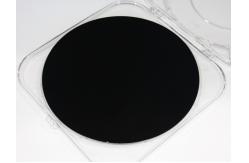
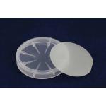
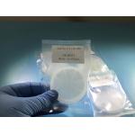
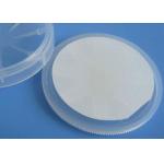
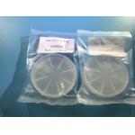
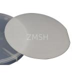
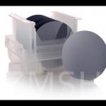
8 Inch AlGaN/GaN Gallium Nitride Wafer For Micro LED
|
|
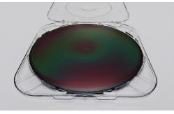
8inch 6inch AlGaN/GaN HEMT-on-HR Si Epiwafer GaN-on-Si Epiwafer for Micro-LED for RF application
GaN Wafer Characteristic
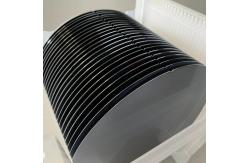
Gallium Nitride is one kind of wide-gap compound semiconductors. Gallium Nitride (GaN) substrate is a high-quality single-crystal substrate. It is made with original HVPE method and wafer processing technology, which has been originally developed for 10+years in China. The features are high crystalline, good uniformity, and superior surface quality. GaN substrates are used for many kinds of applications, for white LED and LD(violet, blue and green) Furthermore, development has progressed for power and high frequency electronic device applications.
Forbidden band width (light emitting and absorption) cover the ultraviolet, visible light and infrared. Application GaN can be used in many areas such as LED display, High-energy
Detection and Imaging,
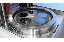
Product specification
Prodcut Specification
ABOUT OUR OEM Factory
Our Factroy Enterprise Vision |
|||||||||||||||||||||||||||||||||||||||||||||||||||||
| Product Tags: GaN Gallium Nitride Wafer Aluminum Nitride Wafer For Micro LED 8 Inch Gallium Arsenide Wafer |
|
2Inch 4inch free-standing GaN Gallium Nitride Wafer |
|
5um Thickness AlN Aluminum Nitride Template 430um Sapphire 350um Sic Substrates |
|
2 4 Inch 4-5 Um III Gallium Nitride Wafer 0.43 Mm Sapphire Sic Substrates |
|
III - Nitride 2 INCH Free Standing GaN Wafer For Laser Projection Display Power Device |
|
2inch 4inch GaN-based Blue Green LED Grown On Flat Or PPS Sapphire MOCVD DSP SSP |
|
8inch GaN-on-Si Epitaxy Wafer 110 111 110 N Type P Type Customization Semiconductor RF LED |