
1 - 10 of 22
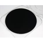
8 inch gallium arsenide wafer
Selling leads
|
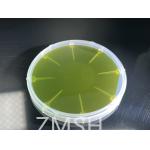
...-doped Gallium arsenide GaAs Wafer Product Description Our 2’’ to 6’’ semi-conducting & semi-insulating GaAs crystal & wafer are wildly used in ...
2025-05-06 20:44:32
|
|
...-doped Gallium arsenide GaAs Wafer Product Description Our 2’’ to 6’’ semi-conducting & semi-insulating GaAs crystal & wafer are wildly used in ...
2025-05-06 20:44:52
|
|
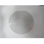
... (GaAs) Gallium Arsenide Wafers Gallium arsenide (GaAs) is a compound of the elements gallium and arsenic. It is a III-V direct bandgap semiconduct...
2025-05-06 20:44:31
|
|
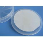
...Gallium arsenide GaAs Wafer Product Description (GaAs) Gallium Arsenide Wafers PWAM Develops and manufactures compound semiconductor substrates...
2025-05-06 20:44:31
|
|
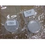
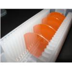
...Inch Silicon Carbide wafer 4H N-Type CVD Orientation : 4.0°±0.5° Semi-Insulating 3-Inch Silicon Carbide wafer's Abstract The unique electronic and ...
2025-05-06 20:41:19
|
|
2inch GaN substrates template,GaN wafer for LeD,semiconducting Gallium Nitride Wafer for ld,GaN template, mocvd GaN Wafer,Free-standing GaN Substrates ...
2025-05-06 20:44:13
|
|
2inch GaN substrates template,GaN wafer for LeD,semiconducting Gallium Nitride Wafer for ld,GaN template, mocvd GaN Wafer,Free-standing GaN Substrates ...
2025-05-06 20:44:29
|
|
2inch 4inch AlN-on-Sapphire Epi-wafer 1-5um AlN template 8inch 6inch AlGaN/GaN HEMT-on-HR Si Epiwafer GaN-on-Si Epiwafer for Micro-LED for RF ...
2025-05-06 20:44:19
|
|
8inch 6inch AlGaN/GaN HEMT-on-HR Si Epiwafer GaN-on-Si Epiwafer for Micro-LED for RF application GaN Wafer Characteristic III-Nitride(GaN,AlN,InN) ...
2025-05-06 20:44:18
|
|
...inch Gallium phosphide (GaP) crystals crystal substrate,GaP wafer ZMKJ can provides 2inch GaP wafer – gallium Phosphide which are grown by LEC...
2025-05-06 20:44:33
|