
11 - 20 of 22
8 inch gallium arsenide wafer
Selling leads
|
2inch R-axis sapphire wafer for epi-ready test ,sapphire optical windows, R-axis 2inch sapphire epi-ready substrate 1. Description Sapphire is one of ...
2025-05-06 20:44:14
|
|
... (GaAs) Gallium Arsenide Wafers Gallium arsenide (GaAs) is a compound of the elements gallium and arsenic. It is a III-V direct bandgap semiconduct...
2025-05-06 20:44:43
|
|
...Inch 153mm 156mm 159mm Thickness 350um 0.5mmt Sapphire Carrier Substrate Wafer SSP DSP Product Description: Sapphire bonding sheet is used for ...
2025-07-30 00:08:00
|
|
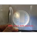
2inch GaN substrates template,GaN wafer for LeD,semiconducting Gallium Nitride Wafer for ld,GaN template, mocvd GaN Wafer,Free-standing GaN Substrates ...
2025-05-06 20:44:28
|
|
2inch GaN substrates template,GaN wafer for LeD, semiconducting Gallium Nitride Wafer for ld, GaN template, mocvd GaN Wafer,Free-standing GaN ...
2025-05-06 20:44:15
|
|
...second-generation semiconductor materials represented by silicon (Si) and gallium arsenide (GaAs) has propelled the swift advancement of microelect...
2025-05-06 20:41:29
|
|
...wafer for epitaxial growth GaAs wafer (Gallium Arsenide) is an advantageous alternative to silicon that has been evolving in the semiconductor ...
2025-05-06 20:44:45
|
|
VGF 2 Inch 4Inch N Type P Type GaAs Wafer Semiconductor Substrate For Epitaxial Growth VGF 2inch 4inch 6inch n-type prime grade GaAs wafer for ...
2025-05-06 20:45:00
|
|
... Substrate Indium Arsenide InAs wafer Application Indium Arsenide (InAs) single crystal semiconductor substrates are materials with unique ...
2025-07-30 00:08:00
|
|
8inch 6inch AlGaN/GaN HEMT-on-HR Si Epiwafer GaN-on-Si Epiwafer for Micro-LED for RF application GaN Wafer Characteristic III-Nitride(GaN,AlN,InN) ...
2025-05-06 20:44:18
|