
6-INCH CONDUCTIVE SINGLE-CRYSTAL SIC ON POLYCRYSTALLINE SIC COMPOSITE SUBSTRATE
|
|
The 6-inch Conductive Single-Crystal SiC on Polycrystalline SiC Composite Substrate
Abstract of the 6-inch Conductive Single-Crystal SiC on Polycrystalline SiC Composite Substrate
The 6-inch conductive single-crystal SiC on polycrystalline SiC composite substrate is a new type of semiconductor substrate structure.
Its core lies in bonding or epitaxially growing a single-crystal conductive SiC thin film onto a polycrystalline silicon carbide (SiC) substrate. This structure combines the high performance of single-crystal SiC (such as high carrier mobility and low defect density) with the low cost and large-size advantages of polycrystalline SiC substrates.
It is suitable for manufacturing high-power, high-frequency devices and is particularly competitive in cost-effective applications. Compared to traditional single-crystal SiC substrates, polycrystalline SiC substrates are prepared via sintering processes, which lowers the cost and allows for larger sizes (such as 6 inches), but their crystal quality is poorer and not suitable for high-performance devices directly.
Attribute Table, Technical Features, and Advantages of The 6-inch Conductive Single-Crystal SiC on Polycrystalline SiC Composite Substrate
Attribute Table
Technical Features, and Advantages
High Conductivity: Single-crystal SiC films achieve low resistivity (<10⁻³ Ω·cm) through doping (e.g., nitrogen doping for n-type), fulfilling low-loss requirements for power devices.
High Thermal Conductivity: SiC has more than three times the thermal conductivity of silicon, enabling effective heat dissipation suitable for high-temperature environments such as EV inverters.
High-Frequency Characteristics: The high electron mobility of single-crystal SiC supports high-frequency switching, including 5G RF devices. Cost and Structural Innovations
Cost Reduction via Polycrystalline Substrates: Polycrystalline SiC substrates are produced by powder sintering, costing only about 1/5 to 1/3 of single-crystal substrates, and scalable to 6 inches or larger sizes.
Heterogeneous Bonding Technology: High-temperature and high-pressure bonding processes achieve atomic-level bonding between single-crystal SiC and the polycrystalline substrate interfaces, avoiding defects common in traditional epitaxial growth.
Improved Mechanical Strength: The high toughness of polycrystalline substrates compensates for the brittleness of single-crystal SiC, enhancing device reliability.
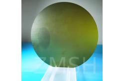
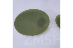
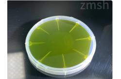
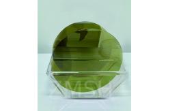
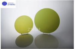
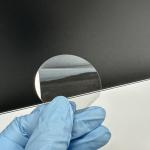
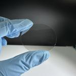
Physical image display
Fabrication Process of the 6-inch Conductive Single-Crystal SiC on Polycrystalline SiC Composite Substrate
Polycrystalline SiC Substrate Preparation: Silicon carbide powder is formed into polycrystalline substrates (~6 inches) via high-temperature sintering.
Single-Crystal SiC Film Growth: Single-crystal SiC layers are epitaxially grown on the polycrystalline substrate using chemical vapor deposition (CVD) or physical vapor transport (PVT).
Bonding Technology: Atomic-level bonding at single-crystal and polycrystalline interfaces is achieved via metal bonding (e.g., silver paste) or direct bonding (DBE).
Annealing Treatment: High-temperature annealing optimizes interface quality and reduces contact resistance.
Core Application Areas of the 6-inch Conductive Single-Crystal SiC on Polycrystalline SiC Composite Substrate
New Energy Vehicles - Main Inverters: Conductive single-crystal SiC MOSFETs improve inverter efficiency (reducing losses by 5% to 10%) and reduce size and weight. - On-Board Chargers (OBC): High-frequency switching characteristics shorten charging times and support 800V high-voltage platforms.
Industrial Power Supply and Photovoltaics - High-Frequency Inverters: Achieve higher conversion efficiency (>98%) in PV systems, reducing overall system cost. - Smart Grids: Reduce energy losses in high-voltage direct current (HVDC) transmission modules.
Aerospace and Defense - Radiation-Hard Devices: Single-crystal SiC’s radiation resistance suits satellite power management modules. - Engine Sensors: High-temperature tolerance (>300°C) simplifies cooling system design.
RF and Communications - 5G Millimeter Wave Devices: Single-crystal SiC-based GaN HEMTs provide high-frequency and high-power output. - Satellite Communications: Polycrystalline substrates’ vibration resistance adapt to harsh space environments.
Q&A
Q:How conductive is a 6-inch conductive single-crystal SiC on a polycrystalline SiC composite substrate?
A:Source of Conductivity: The conductivity of single-crystal SiC is mainly achieved by doping with other elements (such as nitrogen or aluminum). The doping type can be n-type or p-type, resulting in different electrical conductivities and carrier concentrations.
Influence of Polycrystalline SiC: Polycrystalline SiC typically exhibits lower conductivity due to lattice defects and discontinuities affecting its conductive properties. Therefore, in a composite substrate, the polycrystalline portion may have some inhibiting effect on the overall conductivity.
Advantages of the Composite Structure: Combining conductive single-crystal SiC with polycrystalline SiC can potentially improve the overall high-temperature resistance and mechanical strength of the material, while also achieving the desired conductivity through optimized design in certain applications.
Application Potential: This composite structure is often used in high-power electronic devices and high-temperature environments because its excellent thermal and electrical conductivity make it suitable for operation under extreme conditions.
Other Related Product Recommendations
|
||||||||||||||||||||||||||||||||||||
| Product Tags: 6-INCH Silicon Carbide Wafer Single CrystalSilicon Carbide Wafer |
|
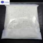
High Purity Semi-Insulating HPSI SiC Powder/99.9999% Purity Crystal Growth |
|
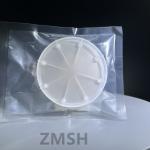
Semi-Insulating SiC Wafers 3inch 76.2mm 4H Type SiC For Semiconductors |
|
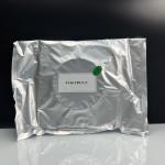
High Resistivity 8inch 200mm Silicon Carbide Wafer Production Grade 4H-N |
|
4H/6H Semi-Insulating Silicon Carbide Wafer For Production/Research/Dummy Grade |
|
Square SiC Windows Silicon Carbide Substrate 1x1x0.5mmt SiC Lens |
|
Semi Insulating Silicon Carbide Wafer SiC Substrate Orientation 0001 Bow/Warp ≤50um |