
Semi-insulating SiC-On-Si Composite Substrates 4H Exhibit High Resistivity LED
|
|
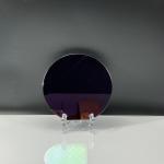
Semi-insulating SiC On Si Composite Substrates 4H Exhibit High Resistivity LED Product Description of SiC On Si Composite Substrates:A semi-insulating silicon carbide (SiC) on silicon compound wafer is a specialized type of wafer that combines the properties of silicon carbide and silicon materials. The wafer consists of a layer of semi-insulating silicon carbide on top of a silicon substrate. The term "semi-insulating" indicates that the material has electrical properties that are not purely conductive or purely insulating, but somewhere in between.
Character of SiC On Si Composite Substrates:
1. High Resistivity: Semi-insulating SiC on Si wafers exhibit high resistivity, which means they have low electrical conductivity compared to regular conductive materials.
Parameter List of SiC On Si Composite Substrates:
Applications of SiC On Si Composite Substrates:1. High-Frequency Devices: Semi-insulating SiC on Si compound wafers are commonly used in high-frequency devices such as RF transistors, amplifiers, and microwave systems.
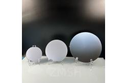
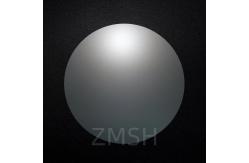
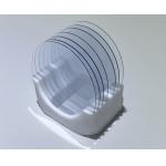
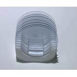
Applications Picture of SiC On Si Composite Substrates:
FAQ:1.Q:What is SiC on Si wafers? A:These wafers are composed of a single crystal of
SiC, a compound semiconductor material where silicon and carbon
atoms form a strong, three-dimensional network. 2.Q:How is SiC compared to Si? A: A key differentiator of SiC over silicon is its
higher system-level efficiency, owing to the greater power density,
lower power loss, higher operating frequency, and increased
temperature operation. A: The use of silicon carbide composite (SiC/SiC) components within fusion reactors has the potential to double the electricity generated from every gigawatt of thermal energy produced compared with advanced steel designs |
||||||||||||||||||||||||||
| Product Tags: LEDs SiC on Si Composite substrates SiC On Si Composite Substrates |
|
Semi Insulating GaN-On-Silicon Wafer Free Standing Gallium Nitride Substrates |
|
1inch 2inch Beta Coefficient Ga2O3 Gallium Oxide Wafer Substrate Dsp Ssp |
|
Beta Coefficient-Ga2O3 Gallium Oxide Wafer Doped Mg Fe3+ Square Substrate Dsp Ssp |

|
Large Thickness SiO2 Thermal Oxide On Silicon Wafers For Optical Communication System |
|
Y-42 Degree 4inch Lithium Tantalate LiTaO3 LiNbO3 Lithium Niobate Crystal Raw Unprocessed Ingots |

|
Single Crystal InP Indium Phosphide Wafers 350 - 650um Thickness |