
Thermal Oxide Layer SiO2 Wafer Thickness 20um MEMS Optical Communication System
|
|
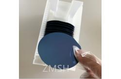
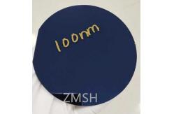
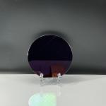
SiO2 wafer Thermal Oxide Laver Thickness 20um+5% MEMS Optical Communication System Product Description:The SIO2 silicon dioxide wafer serves as a foundational element in semiconductor manufacturing. Featuring a thickness ranging from 10μm to 25μm, this crucial substrate is available in 6-inch and 8-inch diameters, ensuring versatility for various applications. Primarily, it acts as an essential insulating layer, playing a pivotal role in microelectronics by providing high dielectric strength. Its refractive index, approximately 1.4458 at 1550nm, ensures optimal performance across diverse applications. Renowned for its uniformity and purity, this wafer stands as an ideal choice for optical devices, integrated circuits, and microelectronics. Its properties facilitate precise device fabrication processes and support technological advancements. Beyond its foundational role in semiconductor manufacturing, it extends its reliability and functionality to a spectrum of applications, guaranteeing stability and efficiency. With its exceptional attributes, the SIO2 silicon dioxide wafer continues to drive innovations in semiconductor technology, enabling advancements in fields such as integrated circuits, optoelectronics, and sensor technologies. Its contributions to cutting-edge technologies underscore its significance as a cornerstone material in the realm of semiconductor production. Features:
Technical Parameters:
Applications:
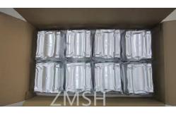
Semiconductor Substrate Brand Name: ZMSH Model Number: Ultra-thick silicon oxide wafer Place of Origin: China Our Semiconductor Substrate is designed with high thermal conductivity, surface oxidation and ultra-thick silicon oxide wafer. It has a thermal conductivity of around 1.4 W/(m·K) @ 300K and melting point of 1,600° C (2,912° F). The boiling point is 2,230° C (4,046° F) and the orientation is <100><11><110>. The molecular weight of this substrate is 60.09. Support and Services:We provide technical support and service for our Semiconductor Substrate product. Our team of experts is available to answer any questions you may have about the product and its features. We can also provide assistance in troubleshooting any issues you encounter while using the product. We also offer remote assistance for those who need it. Our support team is available during normal business hours, and we can be reached by phone, email, or through our website. Packing and Shipping:Packaging and Shipping for Semiconductor Substrate:
FAQ:
|
||||||||||||||||||||||||||||
| Product Tags: Optical Communication System Silicon Dioxide Wafer Thermal Oxide Layer SiO2 Wafer 20um SiO2 Wafer |
|
Semi Insulating GaN-On-Silicon Wafer Free Standing Gallium Nitride Substrates |
|
1inch 2inch Beta Coefficient Ga2O3 Gallium Oxide Wafer Substrate Dsp Ssp |
|
Beta Coefficient-Ga2O3 Gallium Oxide Wafer Doped Mg Fe3+ Square Substrate Dsp Ssp |

|
Large Thickness SiO2 Thermal Oxide On Silicon Wafers For Optical Communication System |
|
Y-42 Degree 4inch Lithium Tantalate LiTaO3 LiNbO3 Lithium Niobate Crystal Raw Unprocessed Ingots |

|
Single Crystal InP Indium Phosphide Wafers 350 - 650um Thickness |