
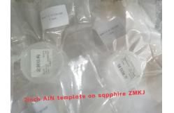
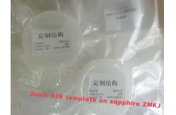
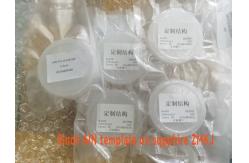
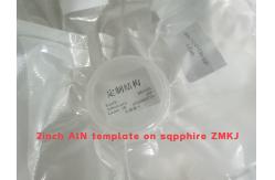
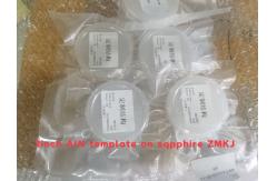
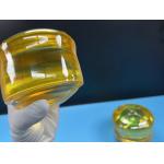
2 Inch Sapphire Substrate AlN Template Layer Wafer For 5G BAW Devices
|
Detailed Product Description
|
2inch 4iinch 6Inch Sapphire based AlN templates AlN film on sapphire substrate 2inch on sapphire substrate AlN Template layer Wafer For 5G BAW Devices
Applications of AlN template Our OEM has developed a serials of proprietary
technologies and the-state-of-the art PVT growth reactors and
facilities to fabricate different sizes of high-quality single crystalline AlN
wafers, AlN temlpates. We are one of the few world-leading high-tech companies who own full AlN fabrication capabilities to
produce high-quality AlN boules and wafers, and provide professional services and turn-key solutions to our
customers,arranged from the growth reactor and hotzone design, modeling and simulation, process design and optimization, crystal
growth, wafering and material characterization. Up to April 2019, they
have applied more than 27 patents (including PCT).
Specification Characteristic Specification
Other relaterd 4INCH GaN Template Specification
|
||||||||||||||||||||||||||||||||||||||||||||||||||||||||||||||||||||
| Product Tags: 2 inch AlN Template 5G BAW Devices AlN Template 2 inch sapphire substrate | ||||||||||||||||||||||||||||||||||||||||||||||||||||||||||||||||||||
Related Products
|
Semi Insulating GaN-On-Silicon Wafer Free Standing Gallium Nitride Substrates |
|
1inch 2inch Beta Coefficient Ga2O3 Gallium Oxide Wafer Substrate Dsp Ssp |
|
Beta Coefficient-Ga2O3 Gallium Oxide Wafer Doped Mg Fe3+ Square Substrate Dsp Ssp |

|
Large Thickness SiO2 Thermal Oxide On Silicon Wafers For Optical Communication System |
|
Y-42 Degree 4inch Lithium Tantalate LiTaO3 LiNbO3 Lithium Niobate Crystal Raw Unprocessed Ingots |

|
Single Crystal InP Indium Phosphide Wafers 350 - 650um Thickness |
Email to this supplier