
11 - 20 of 53
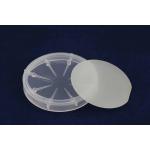
gallium phosphide wafers
Selling leads
|
...wafer for LeD,semiconducting Gallium Nitride Wafer for ld,GaN template, mocvd GaN Wafer,Free-standing GaN Substrates by Customized size,small size ...
2025-05-06 20:44:30
|

|
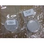
.../3 inch/4 inch 350-650 um InP Crystal Wafer Dummy Prime Semiconductor Substrate Shanghai Xinkehui New Materials Co. Ltd. We specialize in ...
2025-07-24 00:12:37
|
|
...wafer 1-5um AlN template 8inch 6inch AlGaN/GaN HEMT-on-HR Si Epiwafer GaN-on-Si Epiwafer for Micro-LED for RF application GaN Wafer Characteristic ...
2025-05-06 20:44:19
|
|
... Wafer Characteristic III-Nitride(GaN,AlN,InN) Gallium Nitride is one kind of wide-gap compound semiconductors. Gallium Nitride (GaN) substrate is ...
2025-05-06 20:44:18
|
|
2inch R-axis sapphire wafer for epi-ready test ,sapphire optical windows, R-axis 2inch sapphire epi-ready substrate 1. Description Sapphire is one of ...
2025-05-06 20:44:14
|
|
customzied size MPCVD method GaN&Diamond Heat Sink wafers for Thermal management area According to statistics, the temperature of the working junction ...
2025-05-06 20:44:23
|
|
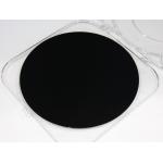
...-doped Gallium arsenide GaAs Wafer Product Description Our 2’’ to 6’’ semi-conducting & semi-insulating GaAs crystal & wafer are wildly used in ...
2025-05-06 20:44:32
|
|
...-doped Gallium arsenide GaAs Wafer Product Description Our 2’’ to 6’’ semi-conducting & semi-insulating GaAs crystal & wafer are wildly used in ...
2025-05-06 20:44:52
|
|
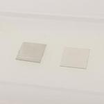
...Phosphide) wafers are renowned for their low defect density and high performance, widely used in optoelectronics and microelectronics. These wafers ...
2025-05-06 20:44:24
|
|
...Phosphide) semiconductor wafers, renowned for their exceptional electronic and optoelectronic properties, have found extensive applications in ...
2025-05-06 20:44:23
|