
41 - 50 of 53
gallium phosphide wafers
Selling leads
|
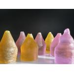
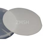
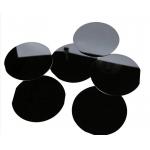
10x10mmt Terbium gallium garnet (TGG)crystals substrate wafer for laser device Product Type: Yttrium aluminum garnet (YAG) is an isotropic crystal ...
2025-07-24 00:12:37
|
|
*, *::before, *::after {box-sizing: border-box;}* {margin: 0;}html, body {height: 100%;}body {line-height: 1.5;-webkit-font-smoothing: antialiased;...
2025-05-06 20:45:37
|
|
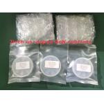
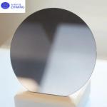
2-4inch Gallium antimonide GaSb Substrate Single Crystal Monocrystal for Semiconductor InAsSb/In-AsPSb, InNAsSb and other heterojunction materials can ...
2025-05-06 20:44:36
|
|
... AlN Wafer Characteristic III-Nitride(GaN,AlN,InN) 2inch AlN template on sapphire or sic substrates, HVPE Gallium Nitride wafer,AlN substrates on ...
2025-05-06 20:44:29
|
|
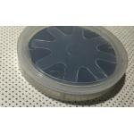
... Blue/Green LED Wafer Flat or PPS Sapphire MOCVD DSP SSP Description of GaN-on-Sapphire Blue/Green LED Wafer: GaN on Sapphire (GaN/Sapphire) wafers ...
2025-05-06 20:44:26
|
|
2inch 4inch 4" 2'' Sapphire based GaN templates GaN film on the sapphire substrate GaN-On-Sapphire GaN wafers GaN substrates GaN windows Properties of ...
2025-05-06 20:44:20
|
|
...wafer for epitaxial growth GaAs wafer (Gallium Arsenide) is an advantageous alternative to silicon that has been evolving in the semiconductor ...
2025-05-06 20:44:45
|
|
...wafers 3inch 4inch N/P TYPE InP Semiconductor Substrate Wafers Doped S+/ Zn+ /Fe + growth (modified VFG method) is used to pull a single crystal ...
2025-05-06 20:44:36
|
|
...wafers 3inch 4inch N/P TYPE InP Semiconductor Substrate Wafers Doped S+/ Zn+ /Fe + growth (modified VFG method) is used to pull a single crystal ...
2025-05-06 20:44:37
|
|
... components used in high-speed optical communication systems, particularly for 2.5 Gbps to 25 Gbps DFB (Distributed Feedback) laser diodes. These ...
2025-05-06 20:45:38
|