
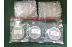
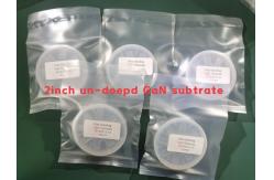
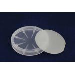
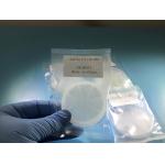
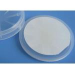
2" Sapphire Based GaN Templates Semiconductor Substrate GaN-On-SiC
|
|
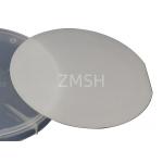
2inch 4inch 4" 2'' Sapphire based GaN templates GaN film on the sapphire substrate GaN-On-Sapphire GaN wafers GaN substrates GaN windows
Properties of GaN 1) At room temperature, GaN is insoluble in water, acid and alkali. 2)Dissolved in a hot alkaline solution at a very slow rate. 3) NaOH, H2SO4 and H3PO4 can quickly corrode the poor quality of GaN, can be used for these poor quality GaN crystal defect detection. 4) GaN in the HCL or hydrogen, at high temperature presents unstable characteristics. 5) GaN is the most stable under nitrogen. Electrical properties of GaN1) The electrical properties of GaN are the most important factors affecting the device. 2) The GaN with no doping was n in all the cases, and the electron concentration of the best sample was about 4*(10^16)/c㎡. 3) Generally, the prepared P samples are highly compensated. Optical Properties Of GaN1) Wide band gap compound semiconductor material with high band width (2.3~6.2eV), can cover the red yellow green, blue, violet and ultraviolet spectrum, so far is that any other semiconductor materials are unable to achieve. 2) Mainly used in blue and violet light emitting device. Properties of GaN Material1) High frequency property, arrive at 300G Hz. (Si is 10G & GaAs is 80G) 2) High temperature property, Normal work at 300℃, very suitable for aerospace, military and other high temperature environment. 3) The electron drift has high saturation velocity, low dielectric constant and good thermal conductivity. 4) Acid and alkali resistance, corrosion resistance, can be used in harsh environment. 5) High voltage characteristics, impact resistance, high reliability. 6) Large power, the communication equipment is very eager. Main Usage Of GaN1) light emitting diodes, LED 2) field effect transistors, FET 3) laser diodes, LD Specification
|
||||||||||||||||||||
| Product Tags: GaN Templates Semiconductor Substrate 2" Sapphire Based Semiconductor Substrate GaN-On-SiC Semiconductor Substrate |
|
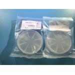
2Inch 4inch free-standing GaN Gallium Nitride Wafer |
|
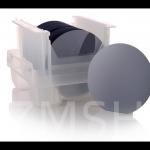
5um Thickness AlN Aluminum Nitride Template 430um Sapphire 350um Sic Substrates |
|
2 4 Inch 4-5 Um III Gallium Nitride Wafer 0.43 Mm Sapphire Sic Substrates |
|
III - Nitride 2 INCH Free Standing GaN Wafer For Laser Projection Display Power Device |
|
2inch 4inch GaN-based Blue Green LED Grown On Flat Or PPS Sapphire MOCVD DSP SSP |
|
8inch GaN-on-Si Epitaxy Wafer 110 111 110 N Type P Type Customization Semiconductor RF LED |