
21 - 30 of 53
gallium phosphide wafers
Selling leads
|
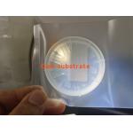
...wafer for LeD,semiconducting Gallium Nitride Wafer for ld,GaN template, mocvd GaN Wafer,Free-standing GaN Substrates by Customized size,small size ...
2025-05-06 20:44:12
|
|
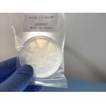
...wafer for LeD,semiconducting Gallium Nitride Wafer for ld,GaN template, mocvd GaN Wafer,Free-standing GaN Substrates by Customized size,small size ...
2025-05-06 20:44:28
|
|
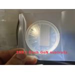
...wafer for LeD, semiconducting Gallium Nitride Wafer for ld, GaN template, mocvd GaN Wafer,Free-standing GaN Substrates by Customized size, small ...
2025-05-06 20:44:15
|
|
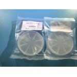
...LED, mocvd Gallium Nitride wafer 10x10mm,5x5mm, 10x5mm GaN wafer,Non-Polar Freestanding GaN Substrates(a-plane and m-plane) 4inch 2inch free...
2025-05-06 20:44:19
|
|
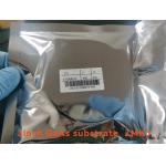
...wafer 2inch with OF Location/Length EJ 0-1-1 / 16±1mm LED LD Mobility Min 100 Product Description: A GaP wafer is a semiconductor substrate ...
2025-05-06 20:45:06
|
|
... Wafer Characteristic III-Nitride(GaN,AlN,InN) Gallium Nitride is one kind of wide-gap compound semiconductors. Gallium Nitride (GaN) substrate is ...
2025-05-06 20:44:18
|
|
...Gallium arsenide GaAs Wafer Product Description (GaAs) Gallium Arsenide Wafers PWAM Develops and manufactures compound semiconductor substrates...
2025-05-06 20:44:31
|
|
... (GaAs) Gallium Arsenide Wafers Gallium arsenide (GaAs) is a compound of the elements gallium and arsenic. It is a III-V direct bandgap semiconduct...
2025-05-06 20:44:31
|
|
... (GaAs) Gallium Arsenide Wafers Gallium arsenide (GaAs) is a compound of the elements gallium and arsenic. It is a III-V direct bandgap semiconduct...
2025-05-06 20:44:43
|
|
...Wafer SSP DSP Product Description: Sapphire bonding sheet is used for thinning and polishing of gallium arsenide wafers Due to the weight and ...
2025-07-24 00:12:37
|