
31 - 40 of 53
gallium phosphide wafers
Selling leads
|
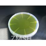
8inch GaN-on-Si Epitaxy Wafer 110 111 110 N-type P-type Customization Semiconductor RF LED Description of GaN-on-Si Wafers: The 8-inch-diameter GaN-on...
2025-05-06 20:44:26
|
|
... innovation. Crafted from pristine indium phosphide, a binary semiconductor renowned for its superior electron velocity, our wafer offers ...
2025-05-06 20:45:10
|
|
2inch/3inch/4inch S/Fe/Zn doped InP Indium Phosphide Single Crystal Wafer Indium phosphide (InP) is an important compound semiconductor material with ...
2025-05-06 20:44:34
|
|
AlN on Diamond template wafers AlN epitaxial films on Diamond substrate AlN on Sapphire /AlN-on-SiC/ AlN-ON Silicon Welcome to Know AlN Template on ...
2025-05-06 20:44:22
|
|
...wafer 4H N-Type CVD Orientation : 4.0°±0.5° Semi-Insulating 3-Inch Silicon Carbide wafer's Abstract The unique electronic and thermal properties of ...
2025-05-06 20:41:19
|
|
...second-generation semiconductor materials represented by silicon (Si) and gallium arsenide (GaAs) has propelled the swift advancement of microelect...
2025-05-06 20:41:29
|
|
...wafer for FP laser diode N-InP substrate FP Epiwafer's Overview Our N-InP Substrate FP Epiwafer is a high-performance epitaxial wafer designed for ...
2025-05-06 20:45:35
|
|
10x10mmt Terbium gallium garnet (TGG)crystals substrate wafer for laser device Product Type: Terbium gallium garnet (TGG) crystal substrateProduct ...
2025-05-06 20:40:28
|
|
... Sapphire Substrate wafers thickness 1.15mm C-a Sapphire application Application Sapphire wafer and substrate applications include: Microelectronic ...
2025-05-06 20:40:27
|
|
VGF 2 Inch 4Inch N Type P Type GaAs Wafer Semiconductor Substrate For Epitaxial Growth VGF 2inch 4inch 6inch n-type prime grade GaAs wafer for ...
2025-05-06 20:45:00
|