
On Diamond Gallium Nitride Wafer Epitaxial HEMT And Bonding
|

|
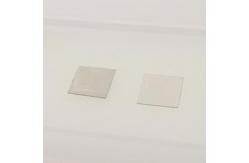
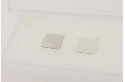
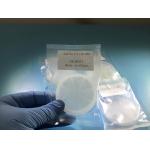
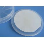
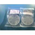
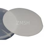
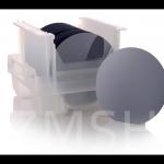
customzied size MPCVD method GaN&Diamond Heat Sink wafers for Thermal management area
According to statistics, the temperature of the working junction
will drop Low 10 ° C can double the device life. The thermal
conductivity of diamond is 3 to 3 higher than that of common
thermal management materials (such as copper, silicon carbide and
aluminum nitride)
On the volume, improve reliability and enhance power density. Once
the "thermal" problem is solved, the semiconductor will also be
significantly improved by effectively improving the performance of
thermal management,
Combination method
Application area • Microwave radio frequency- 5G communication, radar warning, satellite communication and other applications; • Power electronics- smart grid, high-speed rail transit, new energy vehicles, consumer electronics and other applications; Optoelectronics- LED lights, lasers, photodetectors and other applications.
GaN is widely used in radio frequency, fast charging and other fields, but its performance and reliability are related to the temperature on the channel and Joule heating efiect. The commonly used substrate materials (sapphire, silicon, silicon carbide) of GaN-based power devices have low thermal conductivity. It greatly limits the heat dissipation and high-power performance requirements of the device. Relying only on traditional substrate materials (silicon, silicon carbide) and passive cooling technology, it is difficult to meet the heat dissipation requirements under high power conditions, severely limiting the release of the potential of GaN-based power devices. Studies have shown that diamond can significantly improve the use of GaN-based power devices. Existing thermal effect problems. Diamond has wide band gap, high thermal conductivity, high
breakdown field strength, high carrier mobility, high temperature
resistance, acid and alkali resistance, corrosion resistance,
radiation resistance and other superior properties
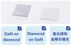
Diamond on GaN We use microwave plasma chemical vapor deposition equipment to achieve epitaxial growth of polycrystalline diamond material with a thickness of <10um on a 50.8 mm(2 inch) silicon-based gallium nitride HEMT. A scanning electron microscope and X-ray diffractometer were used to characterize the surface morphology, crystalline quality, and grain orientation of the diamond film. The results showed that the surface morphology of the sample was relatively uniform, and the diamond grains basically showed a (ill) plane growth. Higher crystal plane orientation. During the growth process, the gallium nitride (GaN) is effectively prevented from being etched by the hydrogen plasma, so that the characteristics of the GaN before and after the diamond coating do not change significantly.
GaN on Diamond In GaN on Diamond epitaxial growth, CSMH uses a special process to grow AlN AIN as the GaN epitaxial layer. CSMH currently has a product available- Epi-ready-GaN on Diamond (AIN on Diamond).
GaN/Diamond bonding The technical indicators of CSMH's diamond heat sink and wafer-level diamond products have reached the world's leading level. The surface roughness of the wafer-level diamond growth surface is Ra<lnm, and the thermal conductivity of the diamond heat sink is 1000_2000W/m.K. By bonding with GaN, the temperature of the device can also be effectively reduced, and the stability and life of the device can be improved.
FAQ & CONTACT
Q:What is your minimum order requirement? Q:How long will it take to execute my order ? Q:Can you give warranty of your products ? Q:How to pay? Q:Can you produce custom optics? |
| Product Tags: GaN On Diamond Wafer Epitaxial HEMT Gallium Nitride Wafer 1mm Diamond GaN Wafer |
|
2Inch 4inch free-standing GaN Gallium Nitride Wafer |
|
5um Thickness AlN Aluminum Nitride Template 430um Sapphire 350um Sic Substrates |
|
2 4 Inch 4-5 Um III Gallium Nitride Wafer 0.43 Mm Sapphire Sic Substrates |
|
III - Nitride 2 INCH Free Standing GaN Wafer For Laser Projection Display Power Device |
|
2inch 4inch GaN-based Blue Green LED Grown On Flat Or PPS Sapphire MOCVD DSP SSP |
|
8inch GaN-on-Si Epitaxy Wafer 110 111 110 N Type P Type Customization Semiconductor RF LED |