
51 - 60 of 147
single wafer shipping containers
Selling leads
|
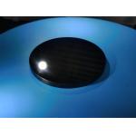
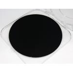
...Wafers SIC Silicon Carbide Wafers Customized High quality high precision Dia.700mm Sic spherical Mirror metal optical reflector Customized High ...
2025-05-06 20:41:05
|
|
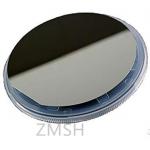
...wafer product is manufactured using advanced Czochralski crystal growth technology and precision cutting and polishing processes, ensuring the ...
2025-05-06 20:41:17
|
|
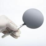
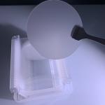
...polished silicon wafer DSP SiO2 wafers Silicon oxide wafer Polished Silicon Wafer High-purity (11N) 1-12 inch single- and double-polished ...
2025-05-06 20:44:47
|
|
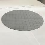
...wafer DSP SiO2 wafers Silicon oxide wafer 1inch 2inch 10x10mm Scanning electron microscope silicon wafer small square piece SEM Polished Silicon ...
2025-05-06 20:44:47
|

|
.../3 inch/4 inch 350-650 um InP Crystal Wafer Dummy Prime Semiconductor Substrate Shanghai Xinkehui New Materials Co. Ltd. We specialize in ...
2025-07-25 00:10:23
|
|
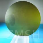
... Wafer Characteristic III-Nitride(GaN,AlN,InN) Gallium Nitride is one kind of wide-gap compound semiconductors. Gallium Nitride (GaN) substrate is ...
2025-05-06 20:44:18
|
|
... Wafer Characteristic III-Nitride(GaN,AlN,InN) Gallium Nitride is one kind of wide-gap compound semiconductors. Gallium Nitride (GaN) substrate is ...
2025-05-06 20:44:18
|
|
...Seed Wafer Thickness 600±50μm Customization Silicon carbide growth Description of SiC Seed Wafer: SiC seed crystal is actually a small crystal with ...
2025-05-06 20:41:47
|
|
..., optoelectronic devices, semiconductor devices, and other fields. The high light transmittance and high hardness of sapphire wafers make them ...
2025-07-25 00:10:23
|
|
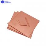
...single crystal Cu wafer 5x5x0.5/lmm 10x10x0.5/1mm 20x20x0.5/1mm a=3.607A Copper substrate's abstract Our copper substrates and wafers are made from ...
2025-05-06 20:45:45
|