
4H SiC Seed Wafer Thickness 600±50μm <1120> Customization Silicon Carbide Growth
|
|
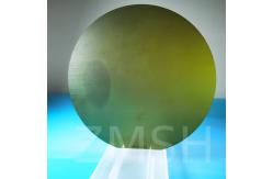
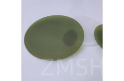
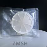
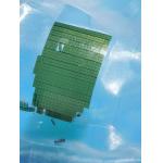
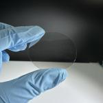
4H SiC Seed Wafer Thickness 600±50μm <1120> Customization Silicon carbide growth Description of SiC Seed Wafer:SiC seed crystal is actually a small crystal with the same crystal orientation as the desired crystal, which serves as the seed for growing a single crystal. It is also known as a crystal seed. By using seed crystals with different crystal orientations, crystals with different orientations can be obtained. Therefore, they are categorized based on their purposes: CZ-pulled single-crystal seed crystals, zone-melting seed crystals, sapphire seed crystals, and SiC seed crystals. In this issue, I will mainly share with you the production process of silicon carbide (SiC) seed crystals, including the selection and preparation of silicon carbide seed crystals, growth methods, thermodynamic properties, growth mechanisms, and growth control. The Character of SiC Seed Wafer:1. Wide band gap 2. High thermal conductivity 3. High critical breakdown field strength 4. High saturation electron drift rate Form of SiC Seed Wafer:
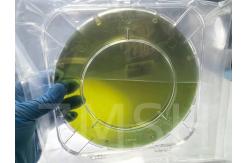
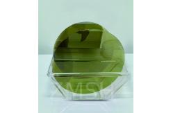
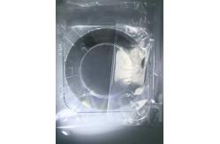
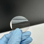
Physical photo of SiC Seed Wafer:Applications of SiC Seed Wafer:The silicon carbide seed crystal is used for preparing silicon carbide. Silicon carbide single crystals are typically grown using the physical vapor transport method. The specific steps of this method involve placing silicon carbide powder at the bottom of a graphite crucible and positioning a silicon carbide seed crystal at the top of the crucible. The graphite crucible is then heated to the sublimation temperature of silicon carbide. The silicon carbide powder decomposes into vapor-phase substances such as Si vapor, Si2C, and SiC2. These substances sublime towards the top of the crucible under the influence of an axial temperature gradient. Upon reaching the top, they condense on the surface of the silicon carbide seed crystal, crystallizing into a silicon carbide single crystal. The diameter of the seed crystal needs to match the desired crystal diameter. During growth, the seed crystal is fixed at the top of the crucible using an adhesive. Application Picture of SiC Seed Wafer:Packing and Shipping:Product Recommend:1.6inch Dia153mm 0.5mm monocrystalline SiC Silicon Carbide crystal seed Wafer or ingot
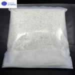
2.4h-N 100um Silicon Carbide Abrasive Powder For SIC Crystal Growth
|
||||||||||||||||||||||||||||||||||
| Product Tags: Silicon Carbide SiC Seed Wafer Customization SiC Seed Wafer SiC Seed Wafer for Growth | ||||||||||||||||||||||||||||||||||
|
High Purity Semi-Insulating HPSI SiC Powder/99.9999% Purity Crystal Growth |
|
Semi-Insulating SiC Wafers 3inch 76.2mm 4H Type SiC For Semiconductors |

|
High Resistivity 8inch 200mm Silicon Carbide Wafer Production Grade 4H-N |
|
4H/6H Semi-Insulating Silicon Carbide Wafer For Production/Research/Dummy Grade |
|
Square SiC Windows Silicon Carbide Substrate 1x1x0.5mmt SiC Lens |
|
Semi Insulating Silicon Carbide Wafer SiC Substrate Orientation 0001 Bow/Warp ≤50um |