
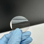
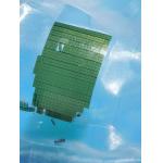
Ultra-Pure Silicon Dark Wafers Semiconductor / Electronic-Grade For Microfabrication
|
Product Description
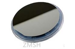
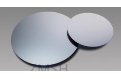
Our high-purity silicon wafer product is manufactured using advanced Czochralski crystal growth technology and precision cutting and polishing processes, ensuring the wafer has extremely high purity and an excellent single-crystal structure. The impurity content is extremely low, meeting the strict standards of the semiconductor manufacturing industry. The surface of the silicon wafer is smooth and flat, with uniform thickness, ensuring high-precision lithography effects in microelectronics manufacturing. In addition, the product exhibits high thermal stability and mechanical strength, maintaining stable performance in high-temperature and high-pressure environments, making it suitable for manufacturing high-performance semiconductor devices. Application
Integrated Circuit Manufacturing: High-purity silicon wafers are the foundational material for manufacturing various integrated circuits, such as microprocessors and memory devices.
Solar Cells: Used to produce high-efficiency solar cells, especially monocrystalline silicon solar cells.
LED Manufacturing: Used in the production of high-brightness, high-efficiency light-emitting diodes (LEDs).
Laser Diodes: Serves as the substrate material for laser diodes used in communications, medical, and industrial applications.
Power Semiconductors: Used to manufacture high-power, high-frequency semiconductor switches and rectifiers.
Sensor Manufacturing: Used as the substrate for manufacturing pressure, temperature, chemical, and biological sensors.
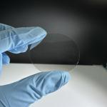
Optical Components: Used to produce various optical components, such as lenses, prisms, and windows.
Feature
Ultra-Pure Silicon Wafers: Emphasizing the exceptionally low level of impurities.
Our Adventages
Exceptional Purity: Our silicon wafers boast an impressive purity level of 99.9999% (6N) or higher, ensuring optimal performance for your applications.
Precision Manufacturing: With stringent quality control, our wafers have precise thickness, orientation, and surface roughness, meeting the highest industry standards.
Versatile Applications: Ideal for a wide range of applications, from semiconductor manufacturing and optoelectronics to high-frequency equipment and micro/nano machining.
High Thermal Conductivity: Our silicon wafers exhibit excellent thermal conductivity, ensuring efficient heat dissipation for your devices.
Robust Physical Properties: With superior bending strength and durability, our wafers provide a reliable foundation for your components.
Customizable Options: We offer customizable options for diameter, thickness, and resistivity to meet your specific requirements.
Ultra-Clean Surface: Our wafers undergo meticulous cleaning processes, resulting in an ultra-clean surface with minimal defects.
Consistent Quality: We adhere to rigorous standards to ensure consistent quality across all our products, giving you peace of mind.
Industry Compliance: Our high-purity silicon wafers comply with industry standards and regulations, ensuring their suitability for various applications. |
||||||||||||||||||||
| Product Tags: Microfabrication Silicon Carbide Wafer Ultra-Pure Silicon Dark Wafers Semiconductor Grade Silicon Dark Wafers |
|
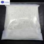
High Purity Semi-Insulating HPSI SiC Powder/99.9999% Purity Crystal Growth |
|
Semi-Insulating SiC Wafers 3inch 76.2mm 4H Type SiC For Semiconductors |
|
High Resistivity 8inch 200mm Silicon Carbide Wafer Production Grade 4H-N |
|
4H/6H Semi-Insulating Silicon Carbide Wafer For Production/Research/Dummy Grade |
|
Square SiC Windows Silicon Carbide Substrate 1x1x0.5mmt SiC Lens |
|
Semi Insulating Silicon Carbide Wafer SiC Substrate Orientation 0001 Bow/Warp ≤50um |