
71 - 80 of 147
single wafer shipping containers
Selling leads
|
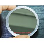
...wafers Ge wafer for microelectronic application N type, Sb doped Ge wafer N type,undoped Ge wafer P type,Ga doped Ge wafer Available size:2”-6” ...
2025-05-06 20:44:46
|
|
SOI Wafer Silicon-on-Insulator Wafer 4inch 5inch 6inch 8inch (100) (111) P Type N Type Description of SOI Wafer: SOI wafer refers to a thin layer of ...
2025-05-06 20:45:41
|
|
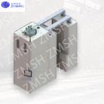
...single crystal SiC Boule growth furnace for 6inch 8inch SiC wafers product SiC Ingot growth Furnace's abstract The SiC Ingot Growth Furnace is an ...
2025-05-06 20:43:53
|
|
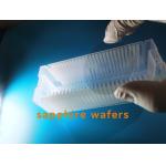
... C-plane DSP Sapphire wafer Why Sapphire? FEATURES OF SINGLE CRYSTAL SAPPHIRE 1. Sapphire has a high optical transmittance, so it is widely used as ...
2025-05-06 20:39:00
|
|
...germanium wafers, which is short for Ge wafers grown by VGF / LEC. Lightly doped P and N-type Germanium wafers can be also used for the Hall effect ...
2025-05-06 20:44:50
|
|
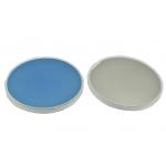
dia50.8mm 2inch 1inch AlN substrate/AlN single crystal wafers 10x10mm or diameter 10mm dia25.4mm dia30mm, dia45mm, dia50.8mm AlN substrate AlN single ...
2025-05-06 20:44:42
|

|
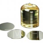
2inch 4inch 6inch Sapphire Wafer Substrate Single Crystal C Miscut A Degree M Plane TTV
2025-05-06 20:39:27
|
|
Dia4inch 100mm 0.43mm 430um Thickness Sapphire Single Crystal Wafer Substrate C-Plane M-Plane 1sp 2sp Product Description: Sapphire Wafer Substrate ...
2025-05-06 20:39:31
|
|
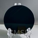
2inch 4inch LiTaO3 Wafer Substrate Double or Single Polished Z-cut X-cut Y-cut Saw grade Description of LiTaO3 Wafer: Lithium tantalate (LiTaO3) has a ...
2025-05-06 20:45:49
|
|
... Wafer Si Substrate 111 P Type N Type for Micro-electromechanical systems (MEMS) Or Power semiconductor devices Or Optical components and sensors ...
2025-05-06 20:45:50
|