
1 - 10 of 271
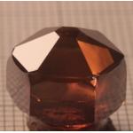
inp crystal semiconductor substrate
Selling leads
|
...film on silicon substrate Applications of AlN template Silicon-based semiconductor technology has reached its limits and could not satisfy the ...
2025-05-06 20:44:41
|
|
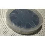
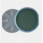
2inch InP wafers 3inch 4inch N/P TYPE InP Semiconductor Substrate Wafers Doped S+/ Zn+ /Fe + growth (modified VFG method) is used to pull a single ...
2025-05-06 20:44:36
|
|
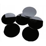
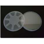
2inch InP wafers 3inch 4inch N/P TYPE InP Semiconductor Substrate Wafers Doped S+/ Zn+ /Fe + growth (modified VFG method) is used to pull a single ...
2025-05-06 20:44:37
|
|
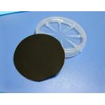
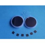
2inch/3inch/4inch S/Fe/Zn doped InP Indium Phosphide Single Crystal Wafer Indium phosphide (InP) is an important compound semiconductor material with ...
2025-05-06 20:44:34
|
|
...variety of applications in the telecommunications, optoelectronics, and semiconductor industries. With superior optical and electronic properties, ...
2025-05-06 20:45:10
|
|
... Substrate Indium Arsenide InAs wafer Application Indium Arsenide (InAs) single crystal semiconductor substrates are materials with unique ...
2025-07-15 00:09:30
|

|
...substrate single crystal Aluminum substrate orientation 111 100 111 5×5×0.5mm a=4.040Ã single crystal Aluminum substrate's brief The demand for ...
2025-05-06 20:45:43
|
|
...semiconductor substrates-gallium arsenide crystal and wafer.We has used advanced crystal growth technology,vertical gradient freeze(VGF) and GaAs ...
2025-05-06 20:44:31
|
|
...substrate, and an infrared light-emitting device with a wavelength of 2 to 14 μm can be fabricated. The AlGaSb superlattice structure material can ...
2025-05-06 20:44:36
|
|
...significant attention in various applications, particularly in the fields of electronics and optoelectronics. This study explores aluminum ...
2025-05-06 20:45:42
|