
81 - 90 of 271
inp crystal semiconductor substrate
Selling leads
|
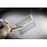
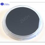
...cut sic wafers SiC windows/lens/glasses About Silicon Carbide (SiC)Crystal Silicon carbide (SiC), also known as carborundum, is a semiconductor ...
2025-05-06 20:40:59
|
|
...cut sic wafers SiC windows/lens/glasses About Silicon Carbide (SiC)Crystal Silicon carbide (SiC), also known as carborundum, is a semiconductor ...
2025-07-16 00:09:36
|
|
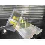
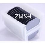
...Substrate/Wafers (150mm, 200mm) Silicon Carbide Ceramic Excellent CorrosionSingle crystal single side polished silicon wafer sic wafer polishing ...
2025-05-06 20:41:07
|
|
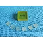
...Substrate 2inch 3inch 4inch 5inch 6inch Un/S/Zn Type N/P DSP/SSP Abstrate of Indium Arsenide (InAs) Substrates Indium Arsenide (InAs) substrates ...
2025-05-27 17:33:17
|
|
...InP (Indium Phosphide) wafers are renowned for their low defect density and high performance, widely used in optoelectronics and microelectronics. ...
2025-05-06 20:44:24
|
|
... crystal substrate Product Name: Zinc oxide (ZnO) crystal substrate Product Description: Zinc oxide (ZnO) crystal substrate is widely used in GaN ...
2025-05-06 20:40:31
|
|
...Crystal substrates by size 10x10x0.5mmt or 2inch x0.5mmt /2'' inch Gadolinium gallium garnet GGG (Gd3Ga5O12) crystal substrate Crystal Substrates ...
2025-05-06 20:40:30
|
|
..., and can obtain a large area substrate (diameter of 2 inches and larger), it is currently an important industrial HTS thin monocrystalline ...
2025-05-06 20:40:34
|
|
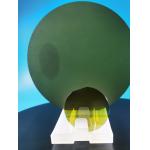
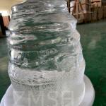
...AL2O3 Monocrystal 80KG 200KG 400KG KY Method LED Semiconductor Describe of Sapphire: Sapphire ingots are aluminum oxide crystals, which are used to ...
2025-05-06 20:40:01
|
|
..., providing high-quality silicon carbide substrates that facilitate cutting-edge semiconductor research and development. 2. Product & Compony ...
2025-05-06 20:45:54
|