
111 - 120 of 271
inp crystal semiconductor substrate
Selling leads
|
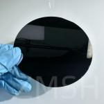
...crystal wafers for High temperature superconducting junction technology Product Name:Strontium titanate (SrTiO 3) crystal substrateProduct ...
2025-05-06 20:40:34
|
|
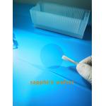
...substrates wafers for GaN epitaxial growth;0.1mm/100um 2inch sapphire c-axis substrates TYPICAL CHOICES FOR PART ORIENTATION: Why Sapphire? Zero ...
2025-05-06 20:38:43
|

|
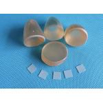
...crystal Dia50.8mm M-axis 2Inch Sapphire Wafers For epitaxial Thickness 500um Double side polished DSP Special Orientation SSP/ DSP A-axis R-axis M...
2025-05-06 20:38:51
|
|
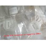
2inch 4iinch 6Inch Sapphire based AlN templates AlN film on sapphire substrate 2inch on sapphire substrate AlN Template layer Wafer For 5G BAW Devices ...
2025-05-06 20:44:44
|
|
8inch GaN-on-Si Epitaxy si substrate(110 111 110)for MOCVD Reactors or RF energy application 8inch GaN-on-Si Epitaxy's abstract The 8-inch GaN-on-Si ...
2025-05-06 20:45:22
|
|
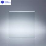
Fluorine Tin Oxide glass FTO coated glass substrate FTO glass1"x1" 1"x3" Transmittance 80~85% Fluorine Tin Oxide glass‘s abstract Fluorine Tin Oxide ...
2025-05-06 20:45:57
|
|
...substrates template,GaN wafer for LeD,semiconducting Gallium Nitride Wafer for ld,GaN template, mocvd GaN Wafer,Free-standing GaN Substrates by ...
2025-05-06 20:44:20
|
|
2inch 50.8mm sapphire DSP wafers thickness 430+/-15um 2inch 430um Ultra Thin sapphire wafers 0.43mm Thickness C-plane/M-plane/A-plane DSP/SSP Sapphire ...
2025-05-06 20:39:14
|
|
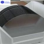
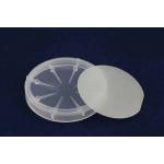
2inch 4inch 6inch 8inch 12inch Si wafer Silicon wafer Polishing Undoped P type N type Semiconductor Description of Si Wafer: Silicon wafer is a ...
2025-05-06 20:45:33
|
|
... Degree: The direction of view is parallel to the optical axis of the crystal 90 Degree: The direction of view is perpendicular to the optical axis ...
2025-05-06 20:38:37
|