
31 - 40 of 271
inp crystal semiconductor substrate
Selling leads
|
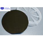
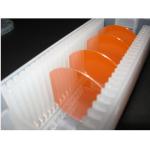
...InP substrate bandwidth 02:2.5G wavelength 1270nm epi wafer for FP laser diode N-InP substrate FP Epiwafer's Overview Our N-InP Substrate FP ...
2025-05-06 20:45:35
|
|
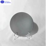
...InP substrate dia 2 3 4 6 inch thickness:350-650um InGaAs doping FP(Fabry-Perot)) Epiwafer InP substrate's abstract Fabry-Perot (FP) Epiwafer on ...
2025-05-06 20:45:36
|
|
... innovation. Crafted from pristine indium phosphide, a binary semiconductor renowned for its superior electron velocity, our wafer offers ...
2025-05-06 20:45:10
|
|
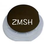
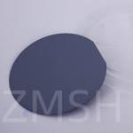
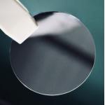
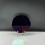
InP wafer 2inch 3inch 4inch VGF P type N type Depant Zn S Fe Undoped Prime Grade Testing Grade *, *::before, *::after {box-sizing: border-box;}* ...
2025-05-06 20:45:30
|
|
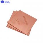
...substrate single crystal Cu wafer 5x5x0.5/lmm 10x10x0.5/1mm 20x20x0.5/1mm a=3.607A Copper substrate's abstract Our copper substrates and wafers are ...
2025-05-06 20:45:45
|
|
... InAs Wafer Crystal Substrates N-Type For MBE 99.9999% Monocrystalline Introduce of InAs substrate Indium InAs or indium mono-arsenide is a ...
2025-05-06 20:44:58
|
|
2-4inch Gallium antimonide GaSb Substrate Single Crystal Monocrystal for Semiconductor Gallium antimonide (GaSb) is a very important III-V direct ...
2025-05-06 20:44:35
|
|
...Wafer with (111) Crystal Orientation – Introduction The 8-inch silicon wafer with (111) crystal orientation is a vital component in the semiconduct...
2025-05-06 20:45:52
|
|
...crystals crystal substrate,GaP wafer ZMKJ can provides 2inch GaP wafer – gallium Phosphide which are grown by LEC(Liquid Encapsulated Czochralski) ...
2025-05-06 20:44:33
|
|
.... Silicon, a semiconductor material, is used to manufacture these wafers due to its excellent electrical properties. Silicon wafers are thin, disk...
2025-05-06 20:45:08
|