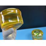
2-4inch Gallium antimonide GaSb Substrate Single Crystal
Monocrystal for Semiconductor
Gallium antimonide (GaSb) is a very important III-V direct bandgap
semiconductor material. It is a key material for Class II
superlattice uncooled medium-long-wave infrared detectors and focal
plane arrays; uncooled medium-long-wave infrared detectors It has
the advantages of long life, light weight, high sensitivity and
high reliability. The product is widely used in infrared lasers,
infrared detectors, infrared sensors and thermal photovoltaic
cells.
The main growth methods of GaSb single crystal materials include
traditional liquid-sealed straight-drawing technology (LEC), mobile
heating/vertical gradient solidification (VGF)/vertical Bridgman
technology.
| 2-4inch or customized |
|
specification |
| single crystal | dope | type | Ion carrier concentration cm-3 | mobility rate (cm2/V.s) | MPD(cm-2) | SIZE |
| GaSb | no | I | (1-2)*1017 | 600-700 | <1*104 | Φ2″×0.5mm Φ3″×0.5mm |
| GaSb | Zn | P | (5-100) *1017 | 200-500 | <1*104 | Φ2″×0.5mm Φ3″×0.5mm |
| GaSb | Te | N | (1-20)*1017 | 2000-3500 | <1*104 | Φ2″×0.5mm Φ3″×0.5mm |
| SIZE(mm) | Dia50.8x0.5mm,10×10×0.5mm,10×5×0.5mmCan be customized |
| Ra | Surface roughness(Ra):<=5A
|
| polish | single or double side polished |
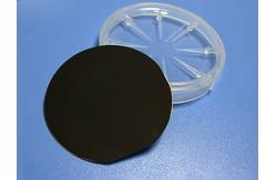
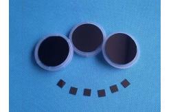
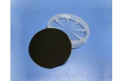
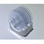
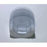
| package | 100 grade cleaning plastic box under 1000 grade cleaning room |
Q: Are you trading company or manufacturer ?
A: zmkj is a trading company but have a sapphire manufacturer
as a supplier of semiconductor materials wafers for a wide span of
applications.
Q: How long is your delivery time?
A: Generally it is 5-10 days if the goods are in stock. or it is
15-20 days if the goods are not
in stock,it is according to quantity.
Q: Do you provide samples ? is it free or extra ?
A: Yes, we could offer the sample for free charge but do not pay
the cost of freight.
Q: What is your terms of payment ?
A: Payment<=1000USD, 100% in advance. Payment>=1000USD,
50% T/T in advance ,balance before shippment.
If you have another question, pls feel free to contact us as below: