
21 - 30 of 271
inp crystal semiconductor substrate
Selling leads
|
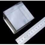
...crystals crystal substrate TeO2 wafer TeO2 Crystal & Q Switch TeO2 is an excellent ascousto-optic (AO) crystal with high AO figure of merit, ...
2025-05-06 20:40:28
|
|
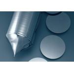
...substrate Ge window for infrared Co2 lasers Ge Material Introduce Among optical materials, germanium materials are increasingly widely used in ...
2025-05-06 20:44:48
|
|
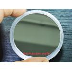
2INCH dia50.8mm Ga doped Ge substrate 4inch N-type 500um Ge wafers Ge wafer for microelectronic application N type, Sb doped Ge wafer N type,undoped ...
2025-05-06 20:44:46
|

|
.../3 inch/4 inch 350-650 um InP Crystal Wafer Dummy Prime Semiconductor Substrate Shanghai Xinkehui New Materials Co. Ltd. We specialize in ...
2025-07-15 00:09:30
|
|
VGF 2inch 4inch 6inch n-type prime grade GaAs wafer for epitaxial growth GaAs wafer (Gallium Arsenide) is an advantageous alternative to silicon that ...
2025-05-06 20:44:45
|
|
2inch N-type single side polished Ge wafers Germanium substrate Ge window for infrared Co2 lasers Diameter:25.4mm Thickness:0.325mm Shanghai Famous ...
2025-05-06 20:44:50
|
|
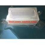
... 3inch 4inch 6inch sapphire substrates wafers for GaN epitaxial growth;0.1mm/100um 2inch sapphire c-axis substrates TYPICAL CHOICES FOR PART ...
2025-05-06 20:38:51
|
|
... solution at a very slow rate. 3) NaOH, H2SO4 and H3PO4 can quickly corrode the poor quality of GaN, can be used for these poor quality GaN crystal ...
2025-05-06 20:44:20
|
|
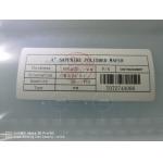
2inch /3inch 4inch /5inch C-axis/ a-axis/ r-axis/ m-axis 6"/6inch dia150mm C-plane Sapphire SSP/DSP wafers with 650um/1000um Thickness About synthetic ...
2025-05-06 20:38:42
|
|
InP DFB Epiwafer wavelength 1390nm InP substrate 2 4 6 inch for 2.5~25G DFB laser diode InP DFB Epiwafer InP substrate's brief InP DFB Epiwafers ...
2025-05-06 20:45:38
|