
11 - 20 of 271
inp crystal semiconductor substrate
Selling leads
|
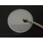
...substrate wafer, LN wafer for saw and optical,SAW Grade LiNbO3 Crystal ingot Description: Lithium niobate (LiNbO3) is a ferroelectric material ...
2025-05-06 20:44:35
|
|
...AlN substrate AlN single crystal wafers Applications of AlN template Silicon-based semiconductor technology has reached its limits and could not ...
2025-05-06 20:44:41
|
|
...substrate Properties of GaN Chemical properties of GaN 1) At room temperature, GaN is insoluble in water, acid and alkali. 2)Dissolved in a hot ...
2025-05-06 20:44:40
|
|
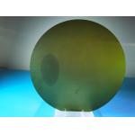
... (GaAs) Gallium Arsenide Wafers Gallium arsenide (GaAs) is a compound of the elements gallium and arsenic. It is a III-V direct bandgap semiconduct...
2025-05-06 20:44:31
|
|
... (GaAs) Gallium Arsenide Wafers Gallium arsenide (GaAs) is a compound of the elements gallium and arsenic. It is a III-V direct bandgap semiconduct...
2025-05-06 20:44:43
|
|
...Semiconductor Substrate For Epitaxial Growth VGF 2inch 4inch 6inch n-type prime grade GaAs wafer for epitaxial growth Gallium arsenide can be made ...
2025-05-06 20:45:00
|
|
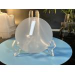
... for 2inch, 4inch, 6inch sapphire substrates and sapphire windows. It is characterized by its extremely low surface roughness (Ra
2025-05-06 20:39:31
|
|
...Substrate/Wafers (150mm, 200mm) Silicon Carbide Ceramic Excellent CorrosionSingle crystal single side polished silicon wafer sic wafer polishing ...
2025-05-06 20:41:07
|
|
... on silicon substrate Applications of AlN template Silicon-based semiconductor technology has reached its limits and could not satisfy the ...
2025-05-06 20:44:38
|
|
... into the ZrO 2 single crystal yttrium (Y) to stabilize its structure, generally the actual use of YSZ single crystal - adding yttrium stabilized ...
2025-05-06 20:40:35
|