
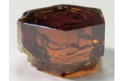
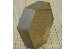
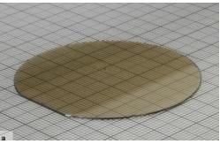
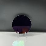
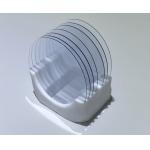
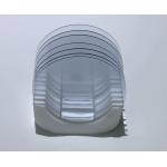
5G Saw Diameter 10mm Single Crystal AlN Semiconductor Substrate
|
Detailed Product Description
|
10x10mm or diameter 10mm dia25.4mm dia30mm, dia45mm, dia50.8mm AlN substrate AlN single crystal wafers
Applications of AlN template Silicon-based semiconductor technology has reached its limits and
could not satisfy the requirements of future electronic devices. As a typical kind of 3rd/4th-generation
semiconductor material, aluminum nitride (AlN) has superior physical and chemical properties such as wide bandgap,
high thermal conductivity, high breakdown filed, high electronic mobility and corrosion/radiation resistance, and is
a perfect substrate for optoelectronic devices, radio frequency (RF) devices, high-power/high-frequency electronic
devices, etc.. Particularly, AlN substrate is the best candidate for UV-LED, UV detectors, UV lasers, 5G
high-power/high-frequency RF devices and 5G SAW/BAW devices, which could widely be used in environmental protection,
electronics, wireless communications, printing, biology, healthcare, military and other fields, such as UV
purification/sterilization, UV curing, photocatalysis, coun terfeit detection, high-density storage, medical phototherapy, drug
discovery, wireless and secure communication, aerospace/deep-space detection and other fields. we have developed a serials of proprietary processes and
technologies to fabricate high-quality AlN templates. At present, Our OEM is the only
company worldwide who can produce 2-6 inch AlN templates in large-scale industrial production capability with
capacity of 300,000 pieces in 2020 to meet explosive market demand from UVC-LED, 5G wireless communication, UV detectors
and sensors etc We currently provide customers with standardized
10x10mm/Φ10mm/Φ15mm/Φ20mm/Φ25.4mm/Φ30mm/Φ50.8mm high quality
nitrogen Aluminum single crystal substrate products, and can also provide customers with 10-20mm non-polar M-plane aluminum nitride single crystal substrate, or customize non-standard 5mm-50.8mm to customers Polished aluminum nitride single crystal substrate. This product is widely used as a high-end substrate material Used in UVC-LED chips, UV detectors, UV lasers, and various high power /High temperature/high frequency electronic device field. Characteristic Specification
Quality Grade S-grade(super) P-grade(production) R-grade(Research)
impurity element C O Si B Na W P S Ti Fe PPMW
27 90 5.4 0.92 0.23 <0.1 <0.1 <0.5 0.46 <0.5
|
||||||||||||||||||||
| Product Tags: diameter 10mm aln substrate 5G saw Semiconductor Substrate single crystal aln substrate |
Related Products
|
Semi Insulating GaN-On-Silicon Wafer Free Standing Gallium Nitride Substrates |
|
1inch 2inch Beta Coefficient Ga2O3 Gallium Oxide Wafer Substrate Dsp Ssp |
|
Beta Coefficient-Ga2O3 Gallium Oxide Wafer Doped Mg Fe3+ Square Substrate Dsp Ssp |

|
Large Thickness SiO2 Thermal Oxide On Silicon Wafers For Optical Communication System |
|
Y-42 Degree 4inch Lithium Tantalate LiTaO3 LiNbO3 Lithium Niobate Crystal Raw Unprocessed Ingots |

|
Single Crystal InP Indium Phosphide Wafers 350 - 650um Thickness |
Email to this supplier